compatibility * Output active low * Low power consumption * Improved immunity against ambient light * Suitable burst length 10 cycles/burst e3 Parts Table Part Carrier Frequency TSOP4830SB1 30 kHz TSOP4833SB1 33 kHz TSOP4836SB1 36 kHz TSOP4837SB1 36.7 kHz TSOP4838SB1 38 kHz TSOP4840SB1 40 kHz TSOP4856SB1 56 kHz Block Diagram Application Circuit 16833 3 16842 1 Input AGC Band Pass Demodulator OUT 2 PIN Control Circuit GND Transmitter TSOPxxxx with TSALxxxx Circuit 30 k VS R1 = 100 VS OUT GND +VS C1 = 4.7 F C VO GND R1 + C1 recommended to suppress power supply disturbances. The output voltage should not be hold continuously at a voltage below VO = 3.3 V by the external circuit. Document Number 82108 Rev. 1.7, 01-Mar-05 www.vishay.com 1 TSOP48..SB1 Vishay Semiconductors Absolute Maximum Ratings Absolute Maximum Ratings Tamb = 25 C, unless otherwise specified Symbol Value Supply Voltage Parameter (Pin 3) Test condition VS - 0.3 to + 6.0 V Supply Current (Pin 3) IS 5 mA Output Voltage (Pin 1) VO - 0.3
 8 Pages, 195 KB, Original
* Output active low * Low power consumption Special Features * Improved immunity against ambient light * Suitable burst length 10 cycles/burst Parts Table Part Carrier Frequency TSOP4830SB1 30 kHz TSOP4833SB1 33 kHz TSOP4836SB1 36 kHz TSOP4837SB1 36.7 kHz TSOP4838SB1 38 kHz TSOP4840SB1 40 kHz TSOP4856SB1 56 kHz Application Circuit Block Diagram 30 k Circuit 3 Transmitter TSOPxxxx with TSALxxxx VS 1 Input AGC Band Pass Demodulator Control Circuit VS +VS C1 = 4.7 F OUT GND C VO GND OUT 2 PIN R1 = 100 GND R1 + C1 recommended to suppress power supply disturbances. The output voltage should not be hold continuously at a voltage below VO = 3.3 V by the external circuit. Absolute Maximum Ratings Tamb = 25 C, unless otherwise specified Parameter Supply Voltage Document Number 82108 Rev. 7, 15-Oct-2002 Test condition (Pin 3) Symbol Value Unit VS - 0.3 to + 6.0 V www.vishay.com 1 TSOP48..SB1 VISHAY Vishay Semiconductors Symbol Value Unit Supply Current Parameter (Pin 3) Test condition IS 5 mA Output Voltag
 7 Pages, 203 KB, Original
TSOP4838SB1 TSOP4856SB1 fo 30 kHz 36 kHz 38 kHz 56 kHz Type TSOP4833SB1 TSOP4837SB1 TSOP4840SB1 fo 33 kHz 36.7 kHz 40 kHz Description The TSOP48..SB1 - series are miniaturized receivers for infrared remote control systems. PIN diode and preamplifier are assembled on lead frame, the epoxy package is designed as IR filter. The demodulated output signal can directly be decoded by a microprocessor. TSOP48..SB1 is the standard IR remote control receiver series, supporting all major transmission codes. 16123 Features D Photo detector and preamplifier in one package D Internal filter for PCM frequency D Improved shielding against electrical field D Low power consumption D High immunity against ambient light D Continuous data transmission possible (800 bit/s) disturbance D Suitable burst length 10 cycles/burst D TTL and CMOS compatibility D Output active low Block Diagram 3 Control Circuit Input 30 kW 1 PIN AGC Band Pass VS OUT Demodulator 2 GND 9612226 Document Number 82108 Rev. 6, 29-Mar-01 www.vishay.
 7 Pages, 182 KB, Original
TSOP4838SB1 TSOP4856SB1 fo 30 kHz 36 kHz 38 kHz 56 kHz Type TSOP4833SB1 TSOP4837SB1 TSOP4840SB1 fo 33 kHz 36.7 kHz 40 kHz Description The TSOP48..SB1 - series are miniaturized receivers for infrared remote control systems. PIN diode and preamplifier are assembled on lead frame, the epoxy package is designed as IR filter. The demodulated output signal can directly be decoded by a microprocessor. The main benefit is the reliable function even in disturbed ambient and the protection against uncontrolled output pulses. 16123 Features D D D D D Special Features Photo detector and preamplifier in one package Internal filter for PCM frequency D Small size package D Enhanced immunity against all kinds of disturbance light TTL and CMOS compatibility D No occurrence of disturbance pulses at Output active low the output Improved shielding against electrical field d isturbance D Short settling time after power on (<200ms) D Suitable burst length 6 cycles/burst Block Diagram 3 Control Circuit Input 30 kW 1 PI
 7 Pages, 144 KB, Original
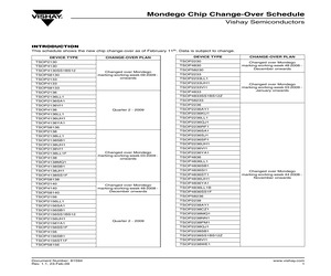
December onwards TSOP2233 TSOP4133 TSOP4136 CHANGE-OVER PLAN www.vishay.com 1 Mondego Chip Change-Over Schedule Vishay Semiconductors DEVICE TYPE CHANGE-OVER PLAN TSOP2238YA1 TSOP2238ZC1 TSOP4838 TSOP4838AY1 TSOP4838DA1 TSOP4838LL1 TSOP4838QJ1 TSOP4838RF1 TSOP4838SB1 TSOP4838SI1 TSOP4838SJ1 TSOP4838SK1AM TSOP4838SO1 TSOP4838SP1 Changed over Mondego marking working week 44 2008 November onwards TSOP4838SS1BS12 TSOP4838SS1BS12Z TSOP4838SS1F TSOP4838ST1 TSOP4838UH1 TSOP4838VI1 TSOP4838YA1 TSOP4838UH1B TSOP4838LL1B TSOP4838YA1B TSOP58238 TSOP2240 TSOP2240RF1 TSOP4840 TSOP4840SB1 Quarter 2 - 2009 TSOP4840SI1 TSOP4840SJ1 TSOP58240 TSOP2256 TSOP2256IV1 TSOP2256SB1 TSOP2256YA1 TSOP4856 Changed over Mondego marking working week 40 2008 October onwards TSOP4856SB1 TSOP58256 www.vishay.com 2 Document Number: 81594 Rev. 1.1, 23-Feb-09
 2 Pages, 16 KB, Original
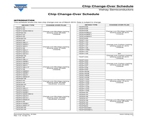
P6236 TSOP6237 Change-over Mondego marking working week 46 2009 - onwards TSOP4838 TSOP4838AY1 TSOP4838DA1 TSOP6238 TSOP4838LL1 TSOP6240 TSOP4838QJ1 TSOP2230 TSOP4830 TSOP58230 Changed-over Mondego marking working week 48 2008 December onwards TSOP4838RF1 TSOP4838SB1 TSOP4838SI1 TSOP2233 TSOP4838SJ1 TSOP2233LL1 TSOP4838SK1AM TSOP2233UH1 TSOP2233VI1 TSOP4833 Change-over Mondego marking working week 03 2009 - January onwards TSOP4838SO1 TSOP4838SP1 TSOP4838SS1BS12Z TSOP58233 TSOP4838SS1F TSOP2236 TSOP4838ST1 TSOP2236AY1 TSOP4838UH1 TSOP2236KU1 TSOP4838VI1 TSOP2236LL1 TSOP4838YA1 TSOP2236QJ1 TSOP4838UH1B TSOP2236RF1 TSOP4838LL1B TSOP2236SA1 TSOP4838YA1B TSOP2236SJ1 TSOP58238 TSOP2236SP1 TSOP2240 TSOP2236UH1 TSOP2240RF1 TSOP2236VI1 TSOP4840 TSOP2236YA1 TSOP4840SB1 TSOP4836 TSOP4840SI1 TSOP4836LL1 TSOP4840SJ1 TSOP4836SB1 TSOP58240 TSOP4836ST1 TSOP4836UH1 Change-over Mondego marking working week 44 2008 - November onwards Change-over Mondego marking working week 44 2008 - November onwards TSOP4838SS1BS
 2 Pages, 19 KB, Original
compatibility * Output active low * Low power consumption * Improved immunity against ambient light * Suitable burst length 10 cycles/burst e3 Parts Table Part Carrier Frequency TSOP4830SB1 30 kHz TSOP4833SB1 33 kHz TSOP4836SB1 36 kHz TSOP4837SB1 36.7 kHz TSOP4838SB1 38 kHz TSOP4840SB1 40 kHz TSOP4856SB1 56 kHz Block Diagram Application Circuit 16833 3 16842 1 Input AGC Band Pass Demodulator OUT 2 PIN Control Circuit GND Transmitter TSOPxxxx with TSALxxxx Circuit 30 k VS R1 = 100 VS OUT GND +VS C1 = 4.7 F C VO GND R1 + C1 recommended to suppress power supply disturbances. The output voltage should not be hold continuously at a voltage below VO = 3.3 V by the external circuit. Document Number 82108 Rev. 1.7, 01-Mar-05 www.vishay.com 1 TSOP48..SB1 Vishay Semiconductors Absolute Maximum Ratings Absolute Maximum Ratings Tamb = 25 C, unless otherwise specified Symbol Value Supply Voltage Parameter (Pin 3) Test condition VS - 0.3 to + 6.0 V Supply Current (Pin 3) IS 5 mA Output Voltage (Pin 1) VO - 0.3
 7 Pages, 172 KB, Original