CK DCKR DCKR DBVR DCKR DBVR DCKR DBVR DCKR DCKR DCKR DBVR 5 5 5 5 5 5 5 5 5 5 5 5 5 5 SN74LVC1G08 SN74LVC1G08 SN74LVC1G08 SN74LVC1G08 SN74LVC1G08 SN74LVC1G08 SN74AHC1G08 SN74AHC1G08 SN74AHCT1G08 SN74AHCT1G08 SN74LVC1G08 SN74AHC1G08 SN74AHC1G08 SN74AHC1G08 SN74LVC1G08DCKR SN74LVC1G08DBVR SN74LVC1G08DCKR SN74LVC1G08DCKR SN74LVC1G08DCKR SN74LVC1G08DBVR SN74AHC1G08DCKR SN74AHC1G08DBVR SN74AHCT1G08DCKR SN74AHCT1G08DBVR SN74LVC1G08DCKR SN74AHC1G08DCKR SN74AHC1G08DCKR SN74AHC1G08DBVR -40 to 125C -40 to 125C -40 to 125C -55 to 125C -55 to 125C -55 to 125C -55 to 125C -55 to 125C -55 to 125C -55 to 125C A-154 Not available in tubes, use DCKR SN74LVC1G06DCKR SN74LVC1G06DBVR SN74LVC1G06DCKR SN74LVC1G06DCKR SN74LVC1G06DCKR HC LVC LVC LVC LVC LX1G LX1G 74V1G 74V1G 74V1T 74V1T LVC HC HC HC Consider the SN74AUC1G06YEAR, lower Vcc range, faster tpd, packages differ This package, consider the SN74LVC1G06YEAR Not available in tubes, use DBVR Consider LVC Little L
 335 Pages, 1395 KB, Original
oot 1G08 1G08 1G08 1G08 1G08 1G08 1G10 1G10 1G11 1G11 Fairchild Orderable NC7ST08P5X NC7SZ08L6X NC7SZ08M5 NC7SZ08M5X NC7SZ08P5 NC7SZ08P5X NC7SZ10P6 NC7SZ10P6X NC7SZ11P6 NC7SZ11P6X TI Orderable SN74AHCT1G08DCKR Not available SN74LVC1G08DBVR SN74LVC1G08DBVR SN74LVC1G08DCKR SN74LVC1G08DCKR Not available Not available Not available Not available Pins 5 6 5 5 5 5 6 6 6 6 1G125 NC7S125M5 SN74AHC1G125DBVR 5 1G125 1G125 1G125 1G125 1G125 1G125 NC7S125M5X NC7SZ125L6X NC7SZ125M5 NC7SZ125M5X NC7SZ125P5 NC7SZ125P5X SN74AHC1G125DBVR Not available SN74LVC1G125DBVR SN74LVC1G125DBVR SN74LVC1G125DCKR SN74LVC1G125DCKR 5 6 5 5 5 5 1G126 NC7S126M5 SN74AHC1G126DBVR 5 1G126 1G126 1G126 1G126 1G126 1G126 1G14 NC7S126M5X NC7SZ126L6X NC7SZ126M5 NC7SZ126M5X NC7SZ126P5 NC7SZ126P5X NC7S14L6X SN74AHC1G126DBVR Not available SN74LVC1G126DBVR SN74LVC1G126DBVR SN74LVC1G126DCKR SN74LVC1G126DCKR Not available 5 6 5 5 5 5 6 1G14 NC7S14M5 SN74AHC1G14DBVR 5 1G14 NC7S14M5X SN74AHC1G14DBVR 5 1G14 NC7S14P5 SN74AHC1G14DCKR 5
 379 Pages, 3043 KB, Original
oot 1G08 1G08 1G08 1G08 1G08 1G08 1G10 1G10 1G11 1G11 Fairchild Orderable NC7ST08P5X NC7SZ08L6X NC7SZ08M5 NC7SZ08M5X NC7SZ08P5 NC7SZ08P5X NC7SZ10P6 NC7SZ10P6X NC7SZ11P6 NC7SZ11P6X TI Orderable SN74AHCT1G08DCKR Not available SN74LVC1G08DBVR SN74LVC1G08DBVR SN74LVC1G08DCKR SN74LVC1G08DCKR Not available Not available Not available Not available Pins 5 6 5 5 5 5 6 6 6 6 1G125 NC7S125M5 SN74AHC1G125DBVR 5 1G125 1G125 1G125 1G125 1G125 1G125 NC7S125M5X NC7SZ125L6X NC7SZ125M5 NC7SZ125M5X NC7SZ125P5 NC7SZ125P5X SN74AHC1G125DBVR Not available SN74LVC1G125DBVR SN74LVC1G125DBVR SN74LVC1G125DCKR SN74LVC1G125DCKR 5 6 5 5 5 5 1G126 NC7S126M5 SN74AHC1G126DBVR 5 1G126 1G126 1G126 1G126 1G126 1G126 1G14 NC7S126M5X NC7SZ126L6X NC7SZ126M5 NC7SZ126M5X NC7SZ126P5 NC7SZ126P5X NC7S14L6X SN74AHC1G126DBVR Not available SN74LVC1G126DBVR SN74LVC1G126DBVR SN74LVC1G126DCKR SN74LVC1G126DCKR Not available 5 6 5 5 5 5 6 1G14 NC7S14M5 SN74AHC1G14DBVR 5 1G14 NC7S14M5X SN74AHC1G14DBVR 5 1G14 NC7S14P5 SN74AHC1G14DCKR 5
 313 Pages, 2889 KB, Original
oot 1G08 1G08 1G08 1G08 1G08 1G08 1G10 1G10 1G11 1G11 Fairchild Orderable NC7ST08P5X NC7SZ08L6X NC7SZ08M5 NC7SZ08M5X NC7SZ08P5 NC7SZ08P5X NC7SZ10P6 NC7SZ10P6X NC7SZ11P6 NC7SZ11P6X TI Orderable SN74AHCT1G08DCKR Not available SN74LVC1G08DBVR SN74LVC1G08DBVR SN74LVC1G08DCKR SN74LVC1G08DCKR Not available Not available Not available Not available Pins 5 6 5 5 5 5 6 6 6 6 1G125 NC7S125M5 SN74AHC1G125DBVR 5 1G125 1G125 1G125 1G125 1G125 1G125 NC7S125M5X NC7SZ125L6X NC7SZ125M5 NC7SZ125M5X NC7SZ125P5 NC7SZ125P5X SN74AHC1G125DBVR Not available SN74LVC1G125DBVR SN74LVC1G125DBVR SN74LVC1G125DCKR SN74LVC1G125DCKR 5 6 5 5 5 5 1G126 NC7S126M5 SN74AHC1G126DBVR 5 1G126 1G126 1G126 1G126 1G126 1G126 1G14 NC7S126M5X NC7SZ126L6X NC7SZ126M5 NC7SZ126M5X NC7SZ126P5 NC7SZ126P5X NC7S14L6X SN74AHC1G126DBVR Not available SN74LVC1G126DBVR SN74LVC1G126DBVR SN74LVC1G126DCKR SN74LVC1G126DCKR Not available 5 6 5 5 5 5 6 1G14 NC7S14M5 SN74AHC1G14DBVR 5 1G14 NC7S14M5X SN74AHC1G14DBVR 5 1G14 NC7S14P5 SN74AHC1G14DCKR 5
 329 Pages, 2106 KB, Original
VC1G08DBVTE4 ACTIVE SOT-23 DBV 5 250 Green (RoHS & no Sb/Br) CU NIPDAU Level-1-260C-UNLIM -40 to 125 SN74LVC1G08DBVTG4 ACTIVE SOT-23 DBV 5 250 Green (RoHS & no Sb/Br) CU NIPDAU Level-1-260C-UNLIM -40 to 125 (C08, C085, C08F, C08K, C08R) (C08H, C08P, C08S) SN74LVC1G08DCKR ACTIVE SC70 DCK 5 3000 Green (RoHS & no Sb/Br) CU NIPDAU | CU SN Level-1-260C-UNLIM -40 to 125 (CE5, CEF, CEK, CE R, CET) (CEH, CEP, CES) SN74LVC1G08DCKRE4 ACTIVE SC70 DCK 5 3000 Green (RoHS & no Sb/Br) CU NIPDAU Level-1-260C-UNLIM -40 to 125 (CE5, CEF, CEK, CE R, CET) (CEH, CEP, CES) SN74LVC1G08DCKRG4 ACTIVE SC70 DCK 5 3000 Green (RoHS & no Sb/Br) CU NIPDAU Level-1-260C-UNLIM -40 to 125 (CE5, CEF, CEK, CE R, CET) (CEH, CEP, CES) SN74LVC1G08DCKT ACTIVE SC70 DCK 5 250 Green (RoHS & no Sb/Br) CU NIPDAU | CU SN Level-1-260C-UNLIM -40 to 125 (CE5, CEF, CEK, CE R, CET) (CEH, CEP, CES) SN74LVC1G08DCKTE4 ACTIVE SC70 DCK 5 250 Green (RoHS & no Sb/Br) CU NIPDAU Level-1-260C-UNLIM -40 to 125 (CE5, CEF, CEK, CE R,
 49 Pages, 2951 KB, Original
eel of 3000 SOT (SC-70) - DCK SOT (SOT-553) - DRL _ _ _CE_ SN74LVC1G08YEPR NanoFree - WCSP (DSBGA) 0.23-mm Large Bump - YZP (Pb-free) SOT (SOT-23) - DBV TOP-SIDE MARKING SN74LVC1G08YZPR Reel of 3000 SN74LVC1G08DBVR Reel of 250 SN74LVC1G08DBVT Reel of 3000 SN74LVC1G08DCKR Reel of 250 SN74LVC1G08DCKT Reel of 4000 SN74LVC1G08DRLR C08_ CE_ Package drawings, standard packing quantities, thermal data, symbolization, and PCB design guidelines are available at www.ti.com/sc/package. DBV/DCK/DRL: The actual top-side marking has one additional character that designates the assembly/test site. YEA/YZA, YEP/YZP: The actual top-side marking has three preceding characters to denote year, month, and sequence code, and one following character to designate the assembly/test site. Pin 1 identifier indicates solder-bump composition (1 = SnPb, * = Pb-free). Please be aware that an important notice concerning availability, standard warranty, and use in critical applications of Texas Instruments semiconductor products
 22 Pages, 724 KB, Original
truments 7 U5,U6 2 SN74LVC1G04DBVR Single inverter gate SOT23-DBV5 ROHS 296-11599-1 Digi-Key Texas Instruments 8 U8 1 SN74LVC244APWR Octal buffer/Driver 3-state outputs TSSOP20-PW ROHS 296-1230-1 Digi-Key Texas Instruments 9 U10, U11, U12, U13, U14, U15 6 SN74LVC1G08DCKR Single 2-Input Positive-and Gate SC70-DCK5 ROHS 296-11602-1 Digi-Key Texas Instruments 10 U2 1 24FC512-I/SM 512k I2C serial EEPROM SOIC8-SM ROHS 24FC512-I/SM Digi-Key Microchip 11 J3 1 TOTX147PL TOSLINKTM Transmitter 3.3V 15MB shutter ROHS 05M1615 NEWARK Toshiba 12 J4 1 TORX147PL(F,T) TOSLINK Receiver 3.3V 15MB shutter ROHS TORX147PLFT Digi-Key Toshiba 13 D1, D2, D4, D5 4 SML-LXT0805YW-TR LED, YELLOW 2.0V SMD0805 ROHS 67-1554-1 Digi-Key Lumex Opto 14 Y1 1 SIT8002AI-13-33E6.00000T Oscillator SMT 6MHz 3.3V Out-enable ROHS 788-8002AI133E6.0T MOUSER 15 Y2 1 ABM10-24.576MHZ-E20-T Crystal SMT-ABM10 24.576MHz 4-pin 10PFD fundamental ROHS 535-9094-1 Digi-Key Abracon 16 C4, C5 2 ECJ-1VC1H470J Capacitor, SMD0603 cerm 47PFD 50V 5% NPO ROHS
 27 Pages, 320 KB, Original
APRIL 1999 - REVISED MARCH 2011 www.ti.com ORDERING INFORMATION Reel of 3000 SN74LVC1G08YZPR _ _ _CE_ SON - DSF Reel of 5000 SN74LVC1G08DSFR CE SON - DRY Reel of 5000 SN74LVC1G08DRYR CE Reel of 3000 SN74LVC1G08DBVR Reel of 250 SN74LVC1G08DBVT Reel of 3000 SN74LVC1G08DCKR Reel of 250 SN74LVC1G08DCKT Reel of 4000 SN74LVC1G08DRLR SOT (SOT-23) - DBV SOT (SC-70) - DCK SOT (SOT-553) - DRL (2) TOP-SIDE MARKING (2) NanoFreeTM - WCSP (DSBGA) 0.23-mm Large Bump - YZP (Pb-free) -40C to 85C (1) ORDERABLE PART NUMBER PACKAGE (1) TA C08_ CE_ Package drawings, standard packing quantities, thermal data, symbolization, and PCB design guidelines are available at www.ti.com/sc/package. DBV/DCK/DRL: The actual top-side marking has one additional character that designates the assembly/test site. YZP: The actual top-side marking has three preceding characters to denote year, month, and sequence code, and one following character to designate the assembly/test site. Pin 1 identifier indicates solder-bump composition (1
 25 Pages, 1058 KB, Original
APRIL 1999 - REVISED MARCH 2011 www.ti.com ORDERING INFORMATION Reel of 3000 SN74LVC1G08YZPR _ _ _CE_ SON - DSF Reel of 5000 SN74LVC1G08DSFR CE SON - DRY Reel of 5000 SN74LVC1G08DRYR CE Reel of 3000 SN74LVC1G08DBVR Reel of 250 SN74LVC1G08DBVT Reel of 3000 SN74LVC1G08DCKR Reel of 250 SN74LVC1G08DCKT Reel of 4000 SN74LVC1G08DRLR SOT (SOT-23) - DBV SOT (SC-70) - DCK SOT (SOT-553) - DRL (2) TOP-SIDE MARKING (2) NanoFreeTM - WCSP (DSBGA) 0.23-mm Large Bump - YZP (Pb-free) -40C to 85C (1) ORDERABLE PART NUMBER PACKAGE (1) TA C08_ CE_ Package drawings, standard packing quantities, thermal data, symbolization, and PCB design guidelines are available at www.ti.com/sc/package. DBV/DCK/DRL: The actual top-side marking has one additional character that designates the assembly/test site. YZP: The actual top-side marking has three preceding characters to denote year, month, and sequence code, and one following character to designate the assembly/test site. Pin 1 identifier indicates solder-bump composition (1
 26 Pages, 1068 KB, Original
APRIL 1999 - REVISED MARCH 2011 www.ti.com ORDERING INFORMATION Reel of 3000 SN74LVC1G08YZPR _ _ _CE_ SON - DSF Reel of 5000 SN74LVC1G08DSFR CE SON - DRY Reel of 5000 SN74LVC1G08DRYR CE Reel of 3000 SN74LVC1G08DBVR Reel of 250 SN74LVC1G08DBVT Reel of 3000 SN74LVC1G08DCKR Reel of 250 SN74LVC1G08DCKT Reel of 4000 SN74LVC1G08DRLR SOT (SOT-23) - DBV SOT (SC-70) - DCK SOT (SOT-553) - DRL (2) TOP-SIDE MARKING (2) NanoFreeTM - WCSP (DSBGA) 0.23-mm Large Bump - YZP (Pb-free) -40C to 85C (1) ORDERABLE PART NUMBER PACKAGE (1) TA C08_ CE_ Package drawings, standard packing quantities, thermal data, symbolization, and PCB design guidelines are available at www.ti.com/sc/package. DBV/DCK/DRL: The actual top-side marking has one additional character that designates the assembly/test site. YZP: The actual top-side marking has three preceding characters to denote year, month, and sequence code, and one following character to designate the assembly/test site. Pin 1 identifier indicates solder-bump composition (1
 23 Pages, 950 KB, Original
een Green Green Green Green Green Green Green Green Green Green Green Green Green Green Green Green Green Orderable Part Number SN74LVC1G06DBVR SN74LVC1G06DCKR SN74LVC1G06DCKR SN74LVC1G07DCKR SN74LVC1G07DCKR SN74LVC1G07DBVR SN74LVC1G07DCKR SN74LVC1G07DCKR SN74LVC1G08DCKR SN74LVC1G08DCKR SN74LVC1G08DBVR SN74LVC1G08DCKR SN74LVC1G08DCKR SN74LVC1G125DCKR SN74LVC1G125DCKR SN74LVC1G125DBVR SN74LVC1G125DCKR SN74LVC1G125DCKR SN74LVC1G126DCKR SN74LVC1G126DCKR SN74LVC1G126DBVR SN74LVC1G126DCKR SN74LVC1G126DCKR SN74LVC1G14DBVR SN74LVC1G14DCKR SN74LVC1G14DCKR SN74LVC1G14DCKR SN74LVC1G14DCKT SN74LVC1G18DBVR SN74LVC1G18DCKR SN74LVC1G18DCKR SN74LVC1G19DBVR SN74LVC1G19DCKR SN74LVC1G19DCKR SN74LVC1G3157DBVR SN74LVC1G3157DBVR SN74LVC1G3157DCKR SN74LVC1G3157DCKR SN74LVC1G32DCKR SN74LVC1G32DCKR SN74LVC1G32DBVR SN74LVC1G32DCKR SN74LVC1G32DCKR SN74LVC1G66DBVR SN74LVC1G66DCKR SN74LVC1G66DCKR SN74LVC1G79DCKR SN74LVC1G79DCKR SN74LVC1G79DBVR SN74LVC1G80DBVR SN74LVC1G79DCKR SN74LVC1G7
 441 Pages, 3298 KB, Original
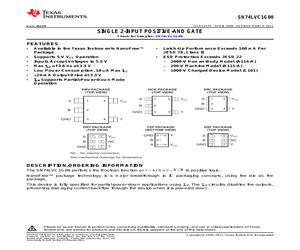
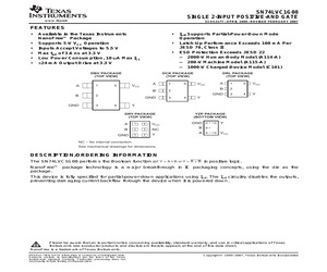
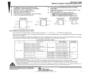
TIVE-AND GATE www.ti.com SCES217T - APRIL 1999 - REVISED FEBRUARY 2007 ORDERING INFORMATION -40C to 85C Reel of 3000 SN74LVC1G08YZPR _ _ _CE_ SON - DRY Reel of 5000 SN74LVC1G08DRYR CE _ Reel of 3000 SN74LVC1G08DBVR Reel of 250 SN74LVC1G08DBVT Reel of 3000 SN74LVC1G08DCKR Reel of 250 SN74LVC1G08DCKT Reel of 4000 SN74LVC1G08DRLR SOT (SOT-23) - DBV SOT (SOT-553) - DRL (2) C08_ CE_ Package drawings, standard packing quantities, thermal data, symbolization, and PCB design guidelines are available at www.ti.com/sc/package. DBV/DCK/DRL/DRY: The actual top-side marking has one additional character that designates the assembly/test site. YZP: The actual top-side marking has three preceding characters to denote year, month, and sequence code, and one following character to designate the assembly/test site. Pin 1 identifier indicates solder-bump composition (1 = SnPb, * = Pb-free). FUNCTION TABLE INPUTS A B OUTPUT Y H H H L X L X L L LOGIC DIAGRAM (POSITIVE LOGIC) 2 TOP-SIDE MARKING (2) NanoFreeTM - WCSP (D
 17 Pages, 620 KB, Original
APRIL 1999 - REVISED MARCH 2011 www.ti.com ORDERING INFORMATION Reel of 3000 SN74LVC1G08YZPR _ _ _CE_ SON - DSF Reel of 5000 SN74LVC1G08DSFR CE SON - DRY Reel of 5000 SN74LVC1G08DRYR CE Reel of 3000 SN74LVC1G08DBVR Reel of 250 SN74LVC1G08DBVT Reel of 3000 SN74LVC1G08DCKR Reel of 250 SN74LVC1G08DCKT Reel of 4000 SN74LVC1G08DRLR SOT (SOT-23) - DBV SOT (SC-70) - DCK SOT (SOT-553) - DRL (2) TOP-SIDE MARKING (2) NanoFreeTM - WCSP (DSBGA) 0.23-mm Large Bump - YZP (Pb-free) -40C to 85C (1) ORDERABLE PART NUMBER PACKAGE (1) TA C08_ CE_ Package drawings, standard packing quantities, thermal data, symbolization, and PCB design guidelines are available at www.ti.com/sc/package. DBV/DCK/DRL: The actual top-side marking has one additional character that designates the assembly/test site. YZP: The actual top-side marking has three preceding characters to denote year, month, and sequence code, and one following character to designate the assembly/test site. Pin 1 identifier indicates solder-bump composition (1
 25 Pages, 1090 KB, Original
eel of 3000 SOT (SC-70) - DCK SOT (SOT-553) - DRL _ _ _CE_ SN74LVC1G08YEPR NanoFree - WCSP (DSBGA) 0.23-mm Large Bump - YZP (Pb-free) SOT (SOT-23) - DBV TOP-SIDE MARKING SN74LVC1G08YZPR Reel of 3000 SN74LVC1G08DBVR Reel of 250 SN74LVC1G08DBVT Reel of 3000 SN74LVC1G08DCKR Reel of 250 SN74LVC1G08DCKT Reel of 4000 SN74LVC1G08DRLR C08_ CE_ Package drawings, standard packing quantities, thermal data, symbolization, and PCB design guidelines are available at www.ti.com/sc/package. DBV/DCK/DRL: The actual top-side marking has one additional character that designates the assembly/test site. YEA/YZA, YEP/YZP: The actual top-side marking has three preceding characters to denote year, month, and sequence code, and one following character to designate the assembly/test site. Pin 1 identifier indicates solder-bump composition (1 = SnPb, * = Pb-free). Please be aware that an important notice concerning availability, standard warranty, and use in critical applications of Texas Instruments semiconductor products
 23 Pages, 796 KB, Original
TIVE-AND GATE www.ti.com SCES217T - APRIL 1999 - REVISED FEBRUARY 2007 ORDERING INFORMATION -40C to 85C Reel of 3000 SN74LVC1G08YZPR _ _ _CE_ SON - DRY Reel of 5000 SN74LVC1G08DRYR CE _ Reel of 3000 SN74LVC1G08DBVR Reel of 250 SN74LVC1G08DBVT Reel of 3000 SN74LVC1G08DCKR Reel of 250 SN74LVC1G08DCKT Reel of 4000 SN74LVC1G08DRLR SOT (SOT-23) - DBV SOT (SOT-553) - DRL (2) C08_ CE_ Package drawings, standard packing quantities, thermal data, symbolization, and PCB design guidelines are available at www.ti.com/sc/package. DBV/DCK/DRL/DRY: The actual top-side marking has one additional character that designates the assembly/test site. YZP: The actual top-side marking has three preceding characters to denote year, month, and sequence code, and one following character to designate the assembly/test site. Pin 1 identifier indicates solder-bump composition (1 = SnPb, * = Pb-free). FUNCTION TABLE INPUTS A B OUTPUT Y H H H L X L X L L LOGIC DIAGRAM (POSITIVE LOGIC) 2 TOP-SIDE MARKING (2) NanoFreeTM - WCSP (D
 17 Pages, 622 KB, Original