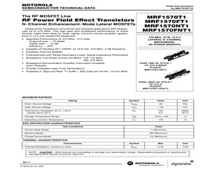
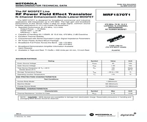
MRF1570T1/D SEMICONDUCTOR TECHNICAL DATA The RF MOSFET Line MRF1570T1 MRF1570FT1 MRF1570NT1 MRF1570FNT1 RF Power Field Effect Transistors N - Channel Enhancement - Mode Lateral MOSFETs Designed for broadband commercial and industrial applications with frequencies up to 470 MHz. The high gain and broadband performance of these devices make them ideal for large - signal, common source amplifier applications in 12.5 volt mobile FM equipment. * Specified Performance @ 470 MHz, 12.5 Volts Output Power -- 70 Watts Power Gain -- 10 dB Efficiency -- 50% * Capable of Handling 20:1 VSWR, @ 15.6 Vdc, 470 MHz, 2 dB Overdrive * Excellent Thermal Stability * Characterized with Series Equivalent Large - Signal Impedance Parameters * Broadband - Full Power Across the Band: 135 - 175 MHz 400 - 470 MHz * Broadband Demonstration Amplifier Information Available Upon Request * N Suffix Indicates Lead - Free Terminations * Available in Tape and Reel. T1 Suffix = 500 Units per 44 mm, 13 inch Reel. 470 MHz,
 20 Pages, 433 KB, Original
MRF1570T1/D SEMICONDUCTOR TECHNICAL DATA The RF MOSFET Line N-Channel Enhancement-Mode Lateral MOSFETs Designed for broadband commercial and industrial applications with frequencies up to 470 MHz. The high gain and broadband performance of these devices make them ideal for large-signal, common source amplifier applications in 12.5 volt mobile FM equipment. * Specified Performance @ 470 MHz, 12.5 Volts Output Power -- 70 Watts Power Gain -- 10 dB Efficiency -- 50% * Capable of Handling 20:1 VSWR, @ 15.6 Vdc, 470 MHz, 2 dB Overdrive * Excellent Thermal Stability * Characterized with Series Equivalent Large-Signal Impedance Parameters * Broadband-Full Power Across the Band: 135-175 MHz 400-470 MHz * Broadband Demonstration Amplifier Information Available Upon Request * Available in Tape and Reel. T1 Suffix = 500 Units per 44 mm, 13 inch Reel. 470 MHz, 70 W, 12.5 V LATERAL N-CHANNEL BROADBAND RF POWER MOSFETs CASE 1366-03, STYLE 1 TO-272 SPLIT LEAD PLASTIC MRF1570T1 CASE 1366A-02, STYLE
 20 Pages, 495 KB, Original
 . . . . . 5-128 MRF18060A . . . . . . . . . . . . . . . . . . . . . . . . . . . . . . . . 5-273 MRF1550FT1 . . . . . . . . . . . . . . . . . . . . . . . . . . . . . . . . 5-128 MRF18060AR3 . . . . . . . . . . . . . . . . . . . . . . . . . . . . . . 5-273 MRF1570T1 . . . . . . . . . . . . . . . . . . . . . . . . . . . . . . . . 5-137 MRF18060ALSR3 . . . . . . . . . . . . . . . . . . . . . . . . . . . 5-273 MRF1570FT1 . . . . . . . . . . . . . . . . . . . . . . . . . . . . . . . . 5-137 MRF18060ASR3 . . . . . . . . . . . . . . . . . . . . . . . . . . . . . 5-273 MRF6522-70 . . . . . . . . . . . . . . . . . . . . . . . . . . . . . . . 5-151 MRF18060B . . . . . . . . . . . . . . . . . . . . . . . . . . . . . . . . 5-279 MRF6522-70R3 . . . . . . . . . . . . . . . . . . . . . . . . . . . . . 5-151 MRF18060BR3 . . . . . . . . . . . . . . . . . . . . . . . . . . . . . . 5-279 MRF9002R2 . . . . . . . . . . . . . . . . . . . . . . . . . . . . . . . . . 5-158 MRF18060BLSR3 . . . . . . . . . . . . . . . . .
 882 Pages, 20361 KB, Original
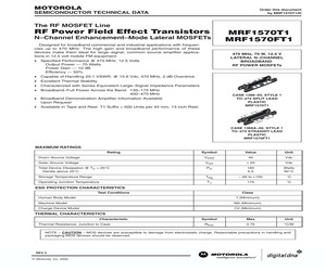
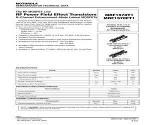
MRF1570T1 Rev. 5, 3/2005 RF Power Field Effect Transistors MRF1570NT1 MRF1570FNT1 MRF1570T1 MRF1570FT1 N-Channel Enhancement-Mode Lateral MOSFETs Designed for broadband commercial and industrial applications with frequencies up to 470 MHz. The high gain and broadband performance of these devices make them ideal for large-signal, common source amplifier applications in 12.5 volt mobile FM equipment. * Specified Performance @ 470 MHz, 12.5 Volts Output Power -- 70 Watts Power Gain -- 10 dB Efficiency -- 50% * Capable of Handling 20:1 VSWR, @ 15.6 Vdc, 470 MHz, 2 dB Overdrive * Excellent Thermal Stability * Characterized with Series Equivalent Large-Signal Impedance Parameters * Broadband-Full Power Across the Band: 135-175 MHz 400-470 MHz * Broadband Demonstration Amplifier Information Available Upon Request * N Suffix Indicates Lead-Free Terminations * 200_C Capable Plastic Package * Available in Tape and Reel. T1 Suffix = 500 Units per 44 mm, 13 inch Reel. 470 MHz, 70 W, 12.5 V LATER
 20 Pages, 401 KB, Original
MRF1570T1/D SEMICONDUCTOR TECHNICAL DATA The RF MOSFET Line N-Channel Enhancement-Mode Lateral MOSFETs Designed for broadband commercial and industrial applications with frequencies up to 470 MHz. The high gain and broadband performance of these devices make them ideal for large-signal, common source amplifier applications in 12.5 volt mobile FM equipment. * Specified Performance @ 470 MHz, 12.5 Volts Output Power -- 70 Watts Power Gain -- 10 dB Efficiency -- 50% * Capable of Handling 20:1 VSWR, @ 15.6 Vdc, 470 MHz, 2 dB Overdrive * Excellent Thermal Stability * Characterized with Series Equivalent Large-Signal Impedance Parameters * Broadband-Full Power Across the Band: 135-175 MHz 400-470 MHz * Broadband Demonstration Amplifier Information Available Upon Request * Available in Tape and Reel. T1 Suffix = 500 Units per 44 mm, 13 inch Reel. 470 MHz, 70 W, 12.5 V LATERAL N-CHANNEL BROADBAND RF POWER MOSFETs CASE 1366-03, STYLE 1 TO-272 SPLIT LEAD PLASTIC MRF1570T1 CASE 1366A-02, STYLE
 20 Pages, 496 KB, Original
MRF1570T1 Rev. 6, 5/2006 Replaced by MRF1570NT1/FNT1. There are no form, fit or function changes with this part replacement. N suffix added to part number to indicate transition to lead - free terminations. MRF1570T1 MRF1570FT1 RF Power Field Effect Transistors Designed for broadband commercial and industrial applications with frequencies up to 470 MHz. The high gain and broadband performance of these devices make them ideal for large - signal, common source amplifier applications in 12.5 volt mobile FM equipment. * Specified Performance @ 470 MHz, 12.5 Volts Output Power -- 70 Watts Power Gain -- 10 dB Efficiency -- 50% * Capable of Handling 20:1 VSWR, @ 15.6 Vdc, 470 MHz, 2 dB Overdrive * Excellent Thermal Stability * Characterized with Series Equivalent Large - Signal Impedance Parameters * Broadband - Full Power Across the Band: 135 - 175 MHz 400 - 470 MHz * Broadband Demonstration Amplifier Information Available Upon Request * 200_C Capable Plastic Package * Available in Tape an
 20 Pages, 431 KB, Original
MRF1570T1/D SEMICONDUCTOR TECHNICAL DATA The RF MOSFET Line N-Channel Enhancement-Mode Lateral MOSFET The MRF1570T1 is designed for broadband commercial and industrial applications with frequencies up to 470 MHz. The high gain and broadband performance of this device make it ideal for large-signal, common source amplifier applications in 12.5 volt mobile FM equipment. * Specified Performance @ 470 MHz, 12.5 Volts Output Power -- 70 Watts Power Gain -- 10 dB Efficiency -- 50% * Capable of Handling 20:1 VSWR, @ 15.6 Vdc, 470 MHz, 2 dB Overdrive * Excellent Thermal Stability * Characterized with Series Equivalent Large-Signal Impedance Parameters * RF Power Plastic Surface Mount Package * Broadband-Full Power Across the Band: 135-175 MHz 400-470 MHz * Broadband Demonstration Amplifier Information Available Upon Request * Available in Tape and Reel. T1 Suffix = 500 Units per 44 mm, 13 inch Reel. 470 MHz, 70 W, 12.5 V LATERAL N-CHANNEL BROADBAND RF POWER MOSFET CASE 1366-01 (TO-272 SPLIT-
 16 Pages, 472 KB, Original
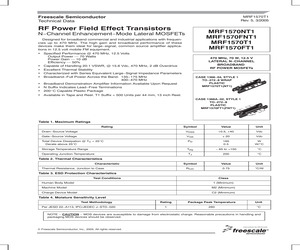
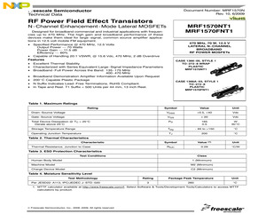
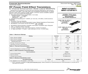
emonstration Amplifier Information Available Upon Request * Available in Tape and Reel. T1 Suffix = 500 Units per 44 mm, 13 inch Reel. !" !" 470 MHz, 70 W, 12.5 V LATERAL N-CHANNEL BROADBAND RF POWER MOSFETs CASE 1366-03, STYLE 1 TO-272 SPLIT LEAD PLASTIC MRF1570T1 CASE 1366A-02, STYLE 1 TO-272 STRAIGHT LEAD PLASTIC MRF1570FT1 MAXIMUM RATINGS Symbol Value Unit Drain-Source Voltage Rating VDSS 40 Vdc Gate-Source Voltage VGS 20 Vdc Total Device Dissipation @ TC = 25C Derate above 25C PD 165 0.5 Watts W/C Storage Temperature Range Tstg - 65 to +150 C Operating Junction Temperature TJ 175 C ESD PROTECTION CHARACTERISTICS Test Conditions Class Human Body Model 1 (Minimum) Machine Model M2 (Minimum) Charge Device Model C2 (Minimum) THERMAL CHARACTERISTICS Characteristic Thermal Resistance, Junction to Case Symbol Max Unit RJC 0.75 C/W NOTE - CAUTION - MOS devices are susceptible to damage from electrostatic charge. Reasonable precautions in handling and packaging MOS devices should be observed. REV 2 M
 14 Pages, 426 KB, Original
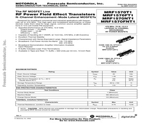
MRF1570T1/D SEMICONDUCTOR TECHNICAL DATA The RF MOSFET Line MRF1570T1 MRF1570FT1 MRF1570NT1 MRF1570FNT1 RF Power Field Effect Transistors Freescale Semiconductor, Inc... N - Channel Enhancement - Mode Lateral MOSFETs Designed for broadband commercial and industrial applications with frequencies up to 470 MHz. The high gain and broadband performance of these devices make them ideal for large - signal, common source amplifier applications in 12.5 volt mobile FM equipment. * Specified Performance @ 470 MHz, 12.5 Volts Output Power -- 70 Watts Power Gain -- 10 dB Efficiency -- 50% * Capable of Handling 20:1 VSWR, @ 15.6 Vdc, 470 MHz, 2 dB Overdrive * Excellent Thermal Stability * Characterized with Series Equivalent Large - Signal Impedance Parameters * Broadband - Full Power Across the Band: 135 - 175 MHz 400 - 470 MHz * Broadband Demonstration Amplifier Information Available Upon Request * N Suffix Indicates Lead - Free Terminations * Available in Tape and Reel. T1 Suffix = 500 Units p
 20 Pages, 628 KB, Original
MRF1570T1 Rev. 6, 5/2006 Replaced by MRF1570NT1/FNT1. There are no form, fit or function changes with this part replacement. N suffix added to part number to indicate transition to lead - free terminations. MRF1570T1 MRF1570FT1 RF Power Field Effect Transistors Designed for broadband commercial and industrial applications with frequencies up to 470 MHz. The high gain and broadband performance of these devices make them ideal for large - signal, common source amplifier applications in 12.5 volt mobile FM equipment. * Specified Performance @ 470 MHz, 12.5 Volts Output Power -- 70 Watts Power Gain -- 10 dB Efficiency -- 50% * Capable of Handling 20:1 VSWR, @ 15.6 Vdc, 470 MHz, 2 dB Overdrive * Excellent Thermal Stability * Characterized with Series Equivalent Large - Signal Impedance Parameters * Broadband - Full Power Across the Band: 135 - 175 MHz 400 - 470 MHz * Broadband Demonstration Amplifier Information Available Upon Request * 200_C Capable Plastic Package * Available in Tape an
 20 Pages, 506 KB, Original
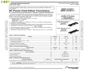
MRF1570T1 MRF1570FT1 N - Channel Enhancement - Mode Lateral MOSFETs Designed for broadband commercial and industrial applications with frequencies up to 470 MHz. The high gain and broadband performance of these devices make them ideal for large - signal, common source amplifier applications in 12.5 volt mobile FM equipment. * Specified Performance @ 470 MHz, 12.5 Volts Output Power -- 70 Watts Power Gain -- 10 dB Efficiency -- 50% * Capable of Handling 20:1 VSWR, @ 15.6 Vdc, 470 MHz, 2 dB Overdrive * Excellent Thermal Stability * Characterized with Series Equivalent Large - Signal Impedance Parameters * Broadband- Full Power Across the Band: 135 - 175 MHz 400 - 470 MHz * Broadband Demonstration Amplifier Information Available Upon Request * N Suffix Indicates Lead - Free Terminations * Available in Tape and Reel. T1 Suffix = 500 Units per 44 mm, 13 inch Reel. 470 MHz, 70 W, 12.5 V LATERAL N - CHANNEL BROADBAND RF POWER MOSFETs CASE 1366 - 04, STYLE 1 TO - 272- 8 WRAP PLASTIC MRF1570T1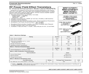 14 Pages, 418 KB, Original
14 Pages, 418 KB, Originalconductor 3 VDD VGG C11 B3 B4 B1 GND C6 C1 C10 L1 C4 C3 C5 L5 C8 R3 R4 C9 L4 L2 C7 C17 C18 C19 C28 C36 C35 C34 C20 C24 R1 L3 C2 GND C37 C38 C12 C13 C14 C33 L9 L7 C30 C26 C22 C23 C31 C27 L10 R2 C15 C32 L8 L6 C29 C42 C41 C40 C21 C25 C44 C43 B5 B6 B2 C16 C39 MRF1570T1 Freescale has begun the transition of marking Printed Circuit Boards (PCBs) with the Freescale Semiconductor signature/logo. PCBs may have either Motorola or Freescale markings during the transition period. These changes will have no impact on form, fit or function of the current product. Figure 2. 135 - 175 MHz Broadband Test Circuit Component Layout TYPICAL CHARACTERISTICS, 135 - 175 MHz 0 IRL, INPUT RETURN LOSS (dB) Pout , OUTPUT POWER (WATTS) 100 80 135 MHz 60 175 MHz 40 150 MHz 20 -5 135 MHz -10 175 MHz 155 MHz -15 VDD = 12.5 Vdc VDD = 12.5 Vdc 0 -20 0 1 2 3 4 5 6 10 20 30 40 50 60 70 80 90 Pin, INPUT POWER (WATTS) Pout, OUTPUT POWER (WATTS) Figure 3. Output Power versus Input Power Figure 4. Input Return Loss versus Output Power
 23 Pages, 612 KB, Original
conductor 3 VDD VGG C11 B3 B4 B1 GND C6 C1 C10 L1 C4 C3 C5 L5 C8 R3 R4 C9 L4 L2 C7 C17 C18 C19 C28 C36 C35 C34 C20 C24 R1 L3 C2 GND C37 C38 C12 C13 C14 C33 L9 L7 C30 C26 C22 C23 C31 C27 L10 R2 C15 C32 L8 L6 C29 C42 C41 C40 C21 C25 C44 C43 B5 B6 B2 C16 C39 MRF1570T1 Freescale has begun the transition of marking Printed Circuit Boards (PCBs) with the Freescale Semiconductor signature/logo. PCBs may have either Motorola or Freescale markings during the transition period. These changes will have no impact on form, fit or function of the current product. Figure 2. 135 - 175 MHz Broadband Test Circuit Component Layout TYPICAL CHARACTERISTICS, 135 - 175 MHz 0 IRL, INPUT RETURN LOSS (dB) Pout , OUTPUT POWER (WATTS) 100 80 135 MHz 60 175 MHz 40 150 MHz 20 -5 135 MHz -10 175 MHz 155 MHz -15 VDD = 12.5 Vdc VDD = 12.5 Vdc 0 -20 0 1 2 3 4 5 6 10 20 30 40 50 60 70 80 90 Pin, INPUT POWER (WATTS) Pout, OUTPUT POWER (WATTS) Figure 3. Output Power versus Input Power Figure 4. Input Return Loss versus Output Power
 23 Pages, 618 KB, Original
conductor 3 VDD VGG C11 B3 B4 B1 GND C6 C1 C10 L1 C4 C3 C5 L5 C8 R3 R4 C9 L4 L2 C7 C17 C18 C19 C28 C36 C35 C34 C20 C24 R1 L3 C2 GND C37 C38 C12 C13 C14 C33 L9 L7 C30 C26 C22 C23 C31 C27 L10 R2 C15 C32 L8 L6 C29 C42 C41 C40 C21 C25 C44 C43 B5 B6 B2 C16 C39 MRF1570T1 Freescale has begun the transition of marking Printed Circuit Boards (PCBs) with the Freescale Semiconductor signature/logo. PCBs may have either Motorola or Freescale markings during the transition period. These changes will have no impact on form, fit or function of the current product. Figure 2. 135 - 175 MHz Broadband Test Circuit Component Layout TYPICAL CHARACTERISTICS, 135 - 175 MHz 0 IRL, INPUT RETURN LOSS (dB) Pout , OUTPUT POWER (WATTS) 100 80 135 MHz 60 175 MHz 40 150 MHz 20 -5 135 MHz -10 175 MHz 155 MHz -15 VDD = 12.5 Vdc VDD = 12.5 Vdc 0 -20 0 1 2 3 4 5 6 10 20 30 40 50 60 70 80 90 Pin, INPUT POWER (WATTS) Pout, OUTPUT POWER (WATTS) Figure 3. Output Power versus Input Power Figure 4. Input Return Loss versus Output Power
 23 Pages, 699 KB, Original
conductor 3 VDD VGG C11 B3 B4 B1 GND C6 C1 C10 L1 C4 C3 C5 L5 C8 R3 R4 C9 L4 L2 C7 C17 C18 C19 C28 C36 C35 C34 C20 C24 R1 L3 C2 GND C37 C38 C12 C13 C14 C33 L9 L7 C30 C26 C22 C23 C31 C27 L10 R2 C15 C32 L8 L6 C29 C42 C41 C40 C21 C25 C44 C43 B5 B6 B2 C16 C39 MRF1570T1 Freescale has begun the transition of marking Printed Circuit Boards (PCBs) with the Freescale Semiconductor signature/logo. PCBs may have either Motorola or Freescale markings during the transition period. These changes will have no impact on form, fit or function of the current product. Figure 2. 135 - 175 MHz Broadband Test Circuit Component Layout TYPICAL CHARACTERISTICS, 135 - 175 MHz 0 IRL, INPUT RETURN LOSS (dB) Pout , OUTPUT POWER (WATTS) 100 80 135 MHz 60 175 MHz 40 150 MHz 20 -5 135 MHz -10 175 MHz 155 MHz -15 VDD = 12.5 Vdc VDD = 12.5 Vdc 0 -20 0 1 2 3 4 5 6 10 20 30 40 50 60 70 80 90 Pin, INPUT POWER (WATTS) Pout, OUTPUT POWER (WATTS) Figure 3. Output Power versus Input Power Figure 4. Input Return Loss versus Output Power
 24 Pages, 619 KB, Original