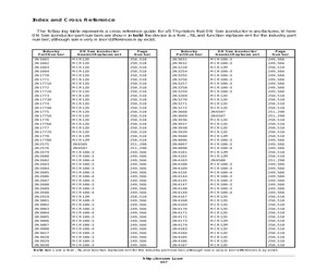
77 Style 2 A K D-PAK Case 369A Style 4 & 5 Surge Current ITSM (Amps) 60 Hz Max IGT (mA) Max VGT (Volts) Data Sheet Page Number in Book 10 0.2 0.8 258 10 0.2 0.8 566 8.0 0.2 0.8 491 15 0.2 0.8 543 20 0.2 0.8 303 25 0.2 1.0 572 25 0.1 0.8 597 25 0.1 0.8 602 MCR08MT1 400 MCR22-6 600 MCR22-8 200 C106B 400 C106D 400 C106D1 600 C106M 600 C106M1 400 MCR106-6 600 MCR106-8 MCR703AT4(2) MCR704AT4(2) 100 200 MCR706AT4(2) MCR708AT4(2) 400 600 4.0 A MCR08BT1 600 1.5 G G G Blocking Voltage VDRM, VRRM (Volts) A Style 5 A On-State RMS Current IT(RMS) (Amps) 0.8 A A MCR716T4(3) MCR718T4(3) 400 600 (1) See TO-92 data sheets for complete device suffix packaging ordering options. RLRA, RLRE, RL, & RL1 suffixes: Radial Tape and Reel RLRM & ZL1 suffixes: Radial Tape and Ammo Pack (2) Denotes pkg style 5 (3) Denotes pkg style 4 Shaded devices denote sensitive gate SCR's http://onsemi.com 249 Lead Identification A = Anode K = Cathode G = Gate SCRs (continued) A A A K A G K A G On-State RMS Current IT(RMS) (Amps) Blockin
 674 Pages, 7097 KB, Original
77 Style 2 A K D-PAK Case 369A Style 4 & 5 Surge Current ITSM (Amps) 60 Hz Max IGT (mA) Max VGT (Volts) Data Sheet Page Number in Book 10 0.2 0.8 258 10 0.2 0.8 566 8.0 0.2 0.8 491 15 0.2 0.8 543 20 0.2 0.8 303 25 0.2 1.0 572 25 0.1 0.8 597 25 0.1 0.8 602 MCR08MT1 400 MCR22-6 600 MCR22-8 200 C106B 400 C106D 400 C106D1 600 C106M 600 C106M1 400 MCR106-6 600 MCR106-8 MCR703AT4(2) MCR704AT4(2) 100 200 MCR706AT4(2) MCR708AT4(2) 400 600 4.0 A MCR08BT1 600 1.5 G G G Blocking Voltage VDRM, VRRM (Volts) A Style 5 K On-State RMS Current IT(RMS) (Amps) 0.8 A A MCR716T4(3) MCR718T4(3) 400 600 (1) See TO-92 data sheets for complete device suffix packaging ordering options. RLRA, RLRE, RL, & RL1 suffixes: Radial Tape and Reel RLRM & ZL1 suffixes: Radial Tape and Ammo Pack (2) Denotes pkg style 4 (3) Denotes pkg style 5 Shaded devices denote sensitive gate SCR's http://onsemi.com 249 Lead Identification A = Anode K = Cathode G = Gate SCRs (continued) A A A K A G K A G On-State RMS Current IT(RMS) (Amps) Blockin
 674 Pages, 7093 KB, Original
C16M MAC15SM MAC16M MAC16M MAC16HCM MAC16N MAC15SN MAC16N MAC16N MAC16HCN MAC15A8FP MAC15A8FP MAC15A8FP MAC15A8FP MAC15A8FP MAC15A8FP MAC15A8FP MAC15A8FP MAC15A10FP MAC15A10FP MAC15A10FP MAC15A10FP MCR25M MCR25M MCR25N MCR106-6 MCR106-8 MCR106-8 MCR708AT4 MCR08MT1 MCR08MT1 MCR08MT1 MCR8SM MCR8SM MCR8SN MCR718T4 MCR718T4 MCR708AT4 MCR708AT4 Page Number Industry Part Number 254, 374 254, 443 254, 443 254, 443 254, 443 254, 443 254, 443 254, 443 254, 443 254, 443 255, 415 254, 404 255, 415 255, 415 255, 420 255, 415 254, 404 255, 415 255, 415 255, 420 255, 415 254, 404 255, 415 255, 415 255, 420 255, 394 255, 394 255, 394 255, 394 255, 394 255, 394 255, 394 255, 394 255, 394 255, 394 255, 394 255, 394 251, 550 251, 550 251, 550 249, 572 249, 572 249, 572 249, 597 249, 491 249, 491 249, 491 250, 514 250, 514 250, 514 249, 602 249, 602 249, 597 249, 597 BT151-500R BT151-650R BT151-800R BT151S-500R BT151S-650R BT151S-800R BT151X-500R BT151X-650R BT151X-800R BT152-400R BT152-60
 14 Pages, 146 KB, Original
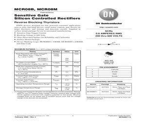
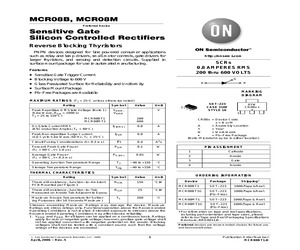
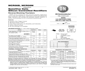
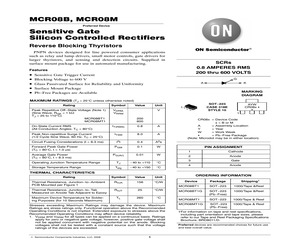
pplied in surface mount package for use in automated manufacturing. * Sensitive Gate Trigger Current * Blocking Voltage to 600 Volts * Glass Passivated Surface for Reliability and Uniformity * Surface Mount Package * Device Marking: Logo, MCR08BT1: CR08B; MCR08MT1: CR08M, and Date Code http://onsemi.com SCRs 0.8 AMPERES RMS 200 thru 600 VOLTS G A K MAXIMUM RATINGS (TJ = 25C unless otherwise noted) Rating Symbol Peak Repetitive Off-State Voltage(1) (Sine Wave, RGK = 1000 , TJ = 25 to 110C) MCR08BT1 MCR08MT1 VDRM, VRRM On-State Current RMS (All Conduction Angles; TC = 80C) IT(RMS) 0.8 Amps ITSM 8.0 Amps Peak Non-repetitive Surge Current (1/2 Cycle Sine Wave, 60 Hz, TC = 25C) Circuit Fusing Considerations (t = 8.3 ms) Value Unit 1 200 600 I2t A2s 0.4 Forward Peak Gate Power (TC = 80C, t = 1.0 s) PGM 0.1 Watts Average Gate Power (TC = 80C, t = 8.3 ms) PG(AV) 0.01 Watts Operating Junction Temperature Range Storage Temperature Range February, 2000 - Rev. 2 2 3 SOT-223 CASE 318E STYLE 10 PI
 12 Pages, 161 KB, Original
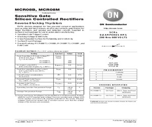
ability and Uniformity Surface Mount Package Pb-Free Packages are Available G A K MARKING DIAGRAM MAXIMUM RATINGS (TJ = 25C unless otherwise noted) Rating Symbol Peak Repetitive Off-State Voltage (Note 1) (Sine Wave, RGK = 1000 W TJ = 25 to 110C) MCR08BT1 MCR08MT1 VDRM, VRRM On-State Current RMS (All Conduction Angles; TC = 80C) IT(RMS) 0.8 A Peak Non-repetitive Surge Current (1/2 Cycle Sine Wave, 60 Hz, TC = 25C) ITSM 8.0 A Circuit Fusing Considerations (t = 8.3 ms) I2t 0.4 A2s PGM 0.1 W Forward Peak Gate Power (TC = 80C, t = 1.0 ms) Average Gate Power (TC = 80C, t = 8.3 ms) Value Unit V 200 600 0.01 W TJ -40 to +110 C Tstg -40 to +150 C Rating Symbol Value Unit Thermal Resistance, Junction-to-Ambient PCB Mounted per Figure 1 RqJA 156 C/W Thermal Resistance, Junction-to-Tab Measured on Anode Tab Adjacent to Epoxy RqJT 25 C/W TL 260 C Storage Temperature Range AYW CR08x G G 1 PG(AV) Operating Junction Temperature Range SOT-223 CASE 318E STYLE 10 1 CR08x = Device Code x = B or M A = Assembly Locat
 6 Pages, 95 KB, Original
Reliability and Uniformity Surface Mount Package Pb-Free Packages are Available G A MARKING DIAGRAM MAXIMUM RATINGS (TJ = 25C unless otherwise noted) Rating Symbol Peak Repetitive Off-State Voltage (Note 1) (Sine Wave, RGK = 1 kW TJ = 25 to 110C) MCR08BT1 MCR08MT1 VDRM, VRRM On-State Current RMS (All Conduction Angles; TC = 80C) IT(RMS) 0.8 A Peak Non-repetitive Surge Current (1/2 Cycle Sine Wave, 60 Hz, TC = 25C) ITSM 8.0 A Circuit Fusing Considerations (t = 8.3 ms) I2t 0.4 A2s PGM 0.1 W Forward Peak Gate Power (TC = 80C, t = 1.0 ms) Average Gate Power (TC = 80C, t = 8.3 ms) Value Unit V 200 600 PG(AV) 0.01 W Operating Junction Temperature Range TJ -40 to +110 C Storage Temperature Range Tstg -40 to +150 C Rating Symbol Value Unit Thermal Resistance, Junction-to-Ambient PCB Mounted per Figure 1 RqJA 156 C/W Thermal Resistance, Junction-to-Tab Measured on Anode Tab Adjacent to Epoxy RqJT 25 C/W TL 260 C THERMAL CHARACTERISTICS Maximum Device Temperature for Soldering Purposes (for 10 Seconds Maxi
 6 Pages, 217 KB, Original
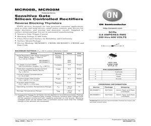
ts. Supplied in surface mount package for use in automated manufacturing. * Sensitive Gate Trigger Current * Blocking Voltage to 600 Volts * Glass Passivated Surface for Reliability and Uniformity * Surface Mount Package * Device Marking: MCR08BT1: CR08B; MCR08MT1: CR08M, and Date Code http://onsemi.com SCRs 0.8 AMPERES RMS 200 thru 600 VOLTS G A K MAXIMUM RATINGS (TJ = 25C unless otherwise noted) Rating Symbol Peak Repetitive Off-State Voltage(1) (Sine Wave, RGK = 1000 , TJ = 25 to 110C) MCR08BT1 MCR08MT1 VDRM, VRRM On-State Current RMS (All Conduction Angles; TC = 80C) IT(RMS) 0.8 Amps ITSM 8.0 Amps Peak Non-repetitive Surge Current (1/2 Cycle Sine Wave, 60 Hz, TC = 25C) Circuit Fusing Considerations (t = 8.3 ms) Value Unit 1 200 600 I2t A2s 0.4 Forward Peak Gate Power (TC = 80C, t = 1.0 s) PGM 0.1 Watts Average Gate Power (TC = 80C, t = 8.3 ms) PG(AV) 0.01 Watts Operating Junction Temperature Range Storage Temperature Range May, 2000 - Rev. 3 2 3 SOT-223 CASE 318E STYLE 10 PIN ASS
 8 Pages, 157 KB, Original
Reliability and Uniformity Surface Mount Package Pb-Free Packages are Available G A MARKING DIAGRAM MAXIMUM RATINGS (TJ = 25C unless otherwise noted) Rating Symbol Peak Repetitive Off-State Voltage (Note 1) (Sine Wave, RGK = 1 kW TJ = 25 to 110C) MCR08BT1 MCR08MT1 VDRM, VRRM On-State Current RMS (All Conduction Angles; TC = 80C) IT(RMS) 0.8 A Peak Non-repetitive Surge Current (1/2 Cycle Sine Wave, 60 Hz, TC = 25C) ITSM 8.0 A Circuit Fusing Considerations (t = 8.3 ms) I2t 0.4 A2s PGM 0.1 W Forward Peak Gate Power (TC = 80C, t = 1.0 ms) Average Gate Power (TC = 80C, t = 8.3 ms) Value Unit V 200 600 PG(AV) 0.01 W Operating Junction Temperature Range TJ -40 to +110 C Storage Temperature Range Tstg -40 to +150 C Rating Symbol Value Unit Thermal Resistance, Junction-to-Ambient PCB Mounted per Figure 1 RqJA 156 C/W Thermal Resistance, Junction-to-Tab Measured on Anode Tab Adjacent to Epoxy RqJT 25 C/W TL 260 C THERMAL CHARACTERISTICS Maximum Device Temperature for Soldering Purposes (for 10 Seconds Maxi
 3 Pages, 115 KB, Original
600 1.5 G G G Blocking Voltage VDRM, VRRM (Volts) A Style 5 A On-State RMS Current IT(RMS) (Amps) 0.8 A A Surge Current ITSM (Amps) 60 Hz Max IGT (mA) Max VGT (Volts) 10 0.2 0.8 10 0.2 0.8 8.0 0.2 0.8 15 0.2 0.8 20 0.2 0.8 25 0.2 1.0 25 0.1 0.8 25 0.1 0.8 MCR08MT1 400 MCR22-6 600 MCR22-8 200 C106B 400 C106D 400 C106D1 600 C106M 600 C106M1 400 MCR106-6 600 MCR106-8 100 MCR703AT4 (Note 2) 200 MCR704AT4 (Note 2) 400 MCR706AT4 (Note 2) 600 MCR708AT4 (Note 2) 400 MCR716T4 (Note 3) 600 MCR718T4 (Note 3) 1. See TO-92 data sheets for complete device suffix packaging ordering options. RLRA, RLRE, RL, & RL1 suffixes: Radial Tape and Reel RLRM & ZL1 suffixes: Radial Tape and Ammo Pack 2. Denotes pkg style 5 3. Denotes pkg style 4 Shaded devices denote sensitive gate SCR's http://onsemi.com 227 Lead Identification A = Anode K = Cathode G = Gate ON Semiconductor Selector Guide - Discrete Devices SCRs (continued) A A A K A G K A G On-State RMS Current IT(RMS) (Amps) Blocking Voltage VDRM, VRRM (Volts) D-PAK Ca
 314 Pages, 1720 KB, Original
ts. Supplied in surface mount package for use in automated manufacturing. * Sensitive Gate Trigger Current * Blocking Voltage to 600 Volts * Glass Passivated Surface for Reliability and Uniformity * Surface Mount Package * Device Marking: MCR08BT1: CR08B; MCR08MT1: CR08M, and Date Code http://onsemi.com SCRs 0.8 AMPERES RMS 200 thru 600 VOLTS G A K MAXIMUM RATINGS (TJ = 25C unless otherwise noted) Rating Symbol Peak Repetitive Off-State Voltage(1) (Sine Wave, RGK = 1000 , TJ = 25 to 110C) MCR08BT1 MCR08MT1 VDRM, VRRM On-State Current RMS (All Conduction Angles; TC = 80C) IT(RMS) 0.8 Amps ITSM 8.0 Amps Peak Non-repetitive Surge Current (1/2 Cycle Sine Wave, 60 Hz, TC = 25C) Circuit Fusing Considerations (t = 8.3 ms) Value Unit I2t A2s 0.4 PGM 0.1 Watts Average Gate Power (TC = 80C, t = 8.3 ms) PG(AV) 0.01 Watts Storage Temperature Range May, 2000 - Rev. 3 2 3 SOT-223 CASE 318E STYLE 10 PIN ASSIGNMENT 1 Cathode 2 Anode 3 Gate 4 Anode ORDERING INFORMATION TJ -40 to +110 C Tstg -40 to +1
 8 Pages, 695 KB, Original
ts. Supplied in surface mount package for use in automated manufacturing. * Sensitive Gate Trigger Current * Blocking Voltage to 600 Volts * Glass Passivated Surface for Reliability and Uniformity * Surface Mount Package * Device Marking: MCR08BT1: CR08B; MCR08MT1: CR08M, and Date Code http://onsemi.com SCRs 0.8 AMPERES RMS 200 thru 600 VOLTS G A K MAXIMUM RATINGS (TJ = 25C unless otherwise noted) Rating Symbol Peak Repetitive Off-State Voltage(1) (Sine Wave, RGK = 1000 , TJ = 25 to 110C) MCR08BT1 MCR08MT1 VDRM, VRRM On-State Current RMS (All Conduction Angles; TC = 80C) IT(RMS) 0.8 Amps ITSM 8.0 Amps Peak Non-repetitive Surge Current (1/2 Cycle Sine Wave, 60 Hz, TC = 25C) Circuit Fusing Considerations (t = 8.3 ms) Value Unit 1 200 600 I2t A2s 0.4 Forward Peak Gate Power (TC = 80C, t = 1.0 s) PGM 0.1 Watts Average Gate Power (TC = 80C, t = 8.3 ms) PG(AV) 0.01 Watts Operating Junction Temperature Range Storage Temperature Range May, 2000 - Rev. 3 2 3 SOT-223 CASE 318E STYLE 10 PIN ASS
 12 Pages, 161 KB, Original
PHASE FREQ DETEC 1 98 5.00 98 B MCK12140DR2 B BBG MECL PHASE FREQ DETEC 1 2500 5.00 2500 B MCK12140DR2G B BBG MECL PHASE FREQ DETEC 1 2500 5.00 2500 B MCR08BT1 A THY S0T223 .8A 200V SCR 2 1000 .187 1000 MCR08BT1G A THY S0T223 .8A 200V SCR 2 1000 .187 1000 MCR08MT1 A THY S0T223 .8A 600V SCR 2 1000 .187 1000 MCR08MT1G A THY S0T223 .8A 600V SCR 2 1000 .187 1000 MCR100-003 A THY T092 .8A 100V SCR 2 5000 .173 5000 MCR100-004 A THY T092 .8A 200V SCR 2 5000 .173 5000 MCR100-006 A THY T092 .8A 400V SCR 2 5000 .173 5000 MCR100-008 A THY T092 .8A 600V SCR 2 5000 .173 5000 MCR100-3RL A THY T092 .8A 100V SCR TR 2 2000 .173 2000 MCR100-3RLG A THY T092 .8A 100V SCR TR 2 2000 .173 2000 MCR100-6G A THY T092 .8A 400V SCR 2 5000 .173 5000 MCR100-6RL A THY T092 .8A 400V SCR TR 2 2000 .173 2000 MCR100-6RLG A THY T092 .8A 400V SCR TR 2 2000 .173 2000 MCR100-6RLRA A THY T092 .8A 400V SCR TR 2 2000 .173 2000 MCR100-6RLRAG A THY T092 .8A 400V SCR TR 2 2000 .173 2000 MCR100-6RLRM A THY T092 .8A 400V SCR TR 2
 296 Pages, 947 KB, Original
AA (TO-126) Case 077 22 D-PAK Case 369A 4 2 5 2 2N5060 34 , ITSM -. 60 Hz 10 2N5061 2N5062 2N5064 MCR100-3 MCR100-4 MCR100-6 MCR100-8 MCR08BT1 56+ IGT (77-) 7- 56+ VGT 1 0.2 0.8 10 0.2 0.8 8.0 0.2 0.8 15 0.2 0.8 20 0.2 0.8 25 0.2 1.0 25 0.1 0.8 25 0.1 0.8 MCR08MT1 MCR22-6 MCR22-8 C106B C106D C106D1 C106M C106M1 MCR106-6 MCR106-8 MCR703AT4 (2) MCR704AT4 (2) MCR706AT4 (2) MCR708AT4 (2) MCR716T4 (3) MCR718T4 (3) (1) ~GJ89 h TO-92 RLRA RLRE RL ! RL1 89 ]b5 RLRM ! ZL1 89 ]b5!? (2) 4 @ (3) 5 @ /JJ SCR http://onsemi.com.cn 252 3 =0 /0 0 - SCR '($ )*+ , IT()*+ )*+) )*+ -. 8.0 8.0 8.0 8.0 8.0 8.0 8.0 8.0 10 12 12 12 12 ' /0 ," VDRM VRRM 1 D-RAK Case 369A 42 600 MCR8DCMT4 800 MCR8DCNT4 TO-220AB Case 221A-09 32 400 MCR8SD 600 MCR8SM 800 MCR8SN 600 MCR8M 800 MCR8N TO-220AB Case 221A-07 32 50 C122F1 200 C122B1 600 MCR8DSMT4 800 MCR8DSNT4 100 MCR72-3 400 MCR72-6 600 MCR72-8 50 MCR218-2 200 MCR218-4 400 MCR218-6 89 TO-220 Case 221C 22 400 MCR218-6FP 800 MCR218-10FP 400 MCR12LD 600 MCR12LM 800 MCR12LN 600 MCR12D
 333 Pages, 7849 KB, Original
E FREQ DETEC 1 2500 5.00 2500 B MCH12140DR2G B BBG MONO PHASE FREQ DETEC 1 2500 5.00 2500 B MCK12140D B BBG MECL PHASE FREQ DETEC 1 98 5.00 98 B MCK12140DR2 B BBG MECL PHASE FREQ DETEC 1 2500 5.00 2500 B MCR08BT1 A THY S0T223 .8A 200V SCR 2 1000 .187 1000 MCR08MT1 A THY S0T223 .8A 600V SCR 2 1000 .187 1000 MCR08MT1G A THY S0T223 .8A 600V SCR 2 1000 .187 1000 MCR100-003 A THY T092 .8A 100V SCR 2 5000 .173 5000 MCR100-004 A THY T092 .8A 200V SCR 2 5000 .173 5000 MCR100-006 A THY T092 .8A 400V SCR 2 5000 .173 5000 MCR100-008 A THY T092 .8A 600V SCR 2 5000 .173 5000 MCR100-3RL A THY T092 .8A 100V SCR TR 2 2000 .173 2000 MCR100-3RLG A THY T092 .8A 100V SCR TR 2 2000 .173 2000 MCR100-6RL A THY T092 .8A 400V SCR TR 2 2000 .173 2000 MCR100-6RLG A THY T092 .8A 400V SCR TR 2 2000 .173 2000 MCR100-6RLRA A THY T092 .8A 400V SCR TR 2 2000 .173 2000 MCR100-6RLRM A THY T092 .8A 400V SCR TR 2 2000 .173 2000 MCR100-6ZL1 A THY T092 0.8A 400V SCR 2 2000 .173 2000 MCR100-8RL A THY T092 0.8A 600V SCR TR
 260 Pages, 833 KB, Original
esistance, Junction-to-Tab Measured on Anode Tab Adjacent to Epoxy RqJT 25 TL 260 Maximum Device Temperature for Soldering Purposes (for 10 Seconds Maximum) October, 2013 - Rev. 7 1 Shipping Device Package C/W MCR08BT1G SOT-223 (Pb-Free) 1000/Tape &Reel C MCR08MT1G SOT-223 (Pb-Free) 1000/Tape & Reel Stresses exceeding Maximum Ratings may damage the device. Maximum Ratings are stress ratings only. Functional operation above the Recommended Operating Conditions is not implied. Extended exposure to stresses above the Recommended Operating Conditions may affect device reliability. 1. VDRM and VRRM for all types can be applied on a continuous basis. Ratings apply for zero or negative gate voltage; however, positive gate voltage shall not be applied concurrent with negative potential on the anode. Blocking voltages shall not be tested with a constant source such that the voltage ratings of the devices are exceeded. (c) Semiconductor Components Industries, LLC, 2013 ORDERING INFORMATION For information
 7 Pages, 143 KB, Original