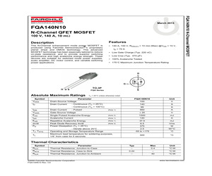
ges that ON Semiconductor was negligent regarding the design or manufacture of the part. ON Semiconductor is an Equal Opportunity/Affirmative Action Employer. This literature is subject to all applicable copyright laws and is not for resale in any manner. FQA140N10 N-Channel QFET(R) MOSFET 100 V, 140 A, 10 m Description This N-Channel enhancement mode power MOSFET is produced using Fairchild Semiconductor's proprietary planar stripe and DMOS technology. This advanced MOSFET technology has been especially tailored to reduce on-state resistance, and to provide superior switching performance and high avalanche energy strength. These devices are suitable for switched mode power supplies, audio amplifier, DC motor control, and variable switching power applications. Features * 140 A, 100 V, RDS(on) = 10 m (Max.) @ VGS = 10 V, ID = 70 A * Low Gate Charge (Typ. 0 nC) * Low Crss (Typ. 470 pF) * 100% Avalanche Tested * 17 D G G D TO-3PN S Absolute Maximum Ratings Symbol VDSS ID S TC = 25C unless otherwise
 10 Pages, 2490 KB, Original
ges that ON Semiconductor was negligent regarding the design or manufacture of the part. ON Semiconductor is an Equal Opportunity/Affirmative Action Employer. This literature is subject to all applicable copyright laws and is not for resale in any manner. FQA140N10 N-Channel QFET(R) MOSFET 100 V, 140 A, 10 m Description This N-Channel enhancement mode power MOSFET is produced using Fairchild Semiconductor's proprietary planar stripe and DMOS technology. This advanced MOSFET technology has been especially tailored to reduce on-state resistance, and to provide superior switching performance and high avalanche energy strength. These devices are suitable for switched mode power supplies, audio amplifier, DC motor control, and variable switching power applications. Features * 140 A, 100 V, RDS(on) = 10 m (Max.) @ VGS = 10 V, ID = 70 A * Low Gate Charge (Typ. 0 nC) * Low Crss (Typ. 470 pF) * 100% Avalanche Tested * 17 D G G D TO-3PN S Absolute Maximum Ratings Symbol VDSS ID S TC = 25C unless otherwise
 10 Pages, 2507 KB, Original
FQA140N10 September 2000 QFET TM FQA140N10 100V N-Channel MOSFET General Description Features These N-Channel enhancement mode power field effect transistors are produced using Fairchild's proprietary, planar stripe, DMOS technology. This advanced technology has been especially tailored to minimize on-state resistance, provide superior switching performance, and withstand high energy pulse in the avalanche and commutation mode. These devices are well suited for low voltage applications such as audio amplifier, high efficiency switching DC/DC converters, and DC motor control. * * * * * * * 140A, 100V, RDS(on) = 0.01 @VGS = 10 V Low gate charge ( typical 220 nC) Low Crss ( typical 470 pF) Fast switching 100% avalanche tested Improved dv/dt capability 175C maximum junction temperature rating D ! " ! " " " G! G DS Absolute Maximum Ratings Symbol VDSS ID TO-3PN ! FQA Series S TC = 25C unless otherwise noted Parameter Drain-Source Voltage - Continuous (TC = 25C) Drain Current FQA140N
 8 Pages, 671 KB, Original
FQA140N10 September 2000 QFET TM FQA140N10 100V N-Channel MOSFET General Description Features These N-Channel enhancement mode power field effect transistors are produced using Fairchild's proprietary, planar stripe, DMOS technology. This advanced technology has been especially tailored to minimize on-state resistance, provide superior switching performance, and withstand high energy pulse in the avalanche and commutation mode. These devices are well suited for low voltage applications such as audio amplifier, high efficiency switching DC/DC converters, and DC motor control. * * * * * * * 140A, 100V, RDS(on) = 0.01 @VGS = 10 V Low gate charge ( typical 220 nC) Low Crss ( typical 470 pF) Fast switching 100% avalanche tested Improved dv/dt capability 175C maximum junction temperature rating D ! " ! " " " G! G DS Absolute Maximum Ratings Symbol VDSS ID TO-3P ! FQA Series S TC = 25C unless otherwise noted Parameter Drain-Source Voltage - Continuous (TC = 25C) Drain Current FQA140N1
 8 Pages, 650 KB, Original
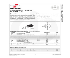
FQA140N10 N-Channel QFET MOSFET 100 V, 140 A, 10 m Description Features This N-Channel enhancement mode power MOSFET is (R) produced using Fairchild Semiconductor 's proprietary planar stripe and DMOS technology. This advanced MOSFET technology has been especially tailored to reduce on-state resistance, and to provide superior switching performance and high avalanche energy strength. These devices are suitable for switched mode power supplies, audio amplifier, DC motor control, and variable switching power applications. * 140 A, 100 V, RDS(on) = 10 m (Max) @VGS = 10 V, ID = 70 A * Low Gate Charge (Typ. 220 nC) * Low Crss (Typ. 470 pF) * 100% Avalanche Tested * 175C Maximum Junction Temperature Rating D G TO-3P G DS ID S FQA Series Absolute Maximum Ratings Symbol VDSS TC = 25C unless otherwise noted Parameter Drain-Source Voltage - Continuous (TC = 25C) Drain Current FQA140N10 100 Unit V 140 A - Continuous (TC = 100C) IDM Drain Current - Pulsed 99 A (Note 1) 560 A 25 V 1500 mJ VGSS Ga
 8 Pages, 856 KB, Original
FQA140N10 N-Channel QFET(R) MOSFET 100 V, 140 A, 10 m Description This N-Channel enhancement mode power MOSFET is produced using Fairchild Semiconductor's proprietary planar stripe and DMOS technology. This advanced MOSFET technology has been especially tailored to reduce on-state resistance, and to provide superior switching performance and high avalanche energy strength. These devices are suitable for switched mode power supplies, audio amplifier, DC motor control, and variable switching power applications. Features * 140 A, 100 V, RDS(on) = 10 m (Max.) @ VGS = 10 V, ID = 70 A * Low Gate Charge (Typ. 0 nC) * Low Crss (Typ. 470 pF) * 100% Avalanche Tested * 17 D G G D TO-3PN S Absolute Maximum Ratings Symbol VDSS ID S TC = 25C unless otherwise noted. Parameter Drain-Source Voltage - Continuous (TC = 25C) Drain Current - Continuous (TC = 100C) FQA140N10 100 Unit V 140 A 99 A (Note 1) 560 A 25 V 1500 mJ IDM Drain Current VGSS Gate-Source Voltage EAS Single Pulsed Avalanche Energy (Not
 9 Pages, 2400 KB, Original
FQA140N10 September 2000 QFET TM FQA140N10 100V N-Channel MOSFET General Description Features These N-Channel enhancement mode power field effect transistors are produced using Fairchild's proprietary, planar stripe, DMOS technology. This advanced technology has been especially tailored to minimize on-state resistance, provide superior switching performance, and withstand high energy pulse in the avalanche and commutation mode. These devices are well suited for low voltage applications such as audio amplifier, high efficiency switching DC/DC converters, and DC motor control. * * * * * * * 140A, 100V, RDS(on) = 0.01 @VGS = 10 V Low gate charge ( typical 220 nC) Low Crss ( typical 470 pF) Fast switching 100% avalanche tested Improved dv/dt capability 175C maximum junction temperature rating D ! " ! " " " G! G DS Absolute Maximum Ratings Symbol VDSS ID TO-3PN ! FQA Series S TC = 25C unless otherwise noted Parameter Drain-Source Voltage - Continuous (TC = 25C) Drain Current FQA140N
 8 Pages, 679 KB, Original
oad Switching and Inrush Control By adding a second MOSFET as shown in Figure 6, the LTC4359 can be used to control power flow in the forward direction while retaining ideal diode behavior in the reverse direction. The body diodes of Q1 and Q2 prohibit Q2 FQA140N10 VIN 28V ON OFF Q1 FDMS86101 VOUT 28V 10A D1 SMAJ58A 58V D2 SMAJ24A 24V R1A 1k VINB = 12V If the other, initially lower, supply was not delivering any load current at the time of the fault, the output falls until the body diode of its ORing MOSFET conducts. Mean-while, the LTC4359 charges the MOSFET gate with 10A until the forward drop is reduced to 30mV. If this supply was sharing load current at the time of the fault, its associated ORing MOSFET was already driven partially on. In this case, the LTC4359 will simply drive the MOSFET gate harder in an effort to maintain a drop of 30mV. 12V 10A BUS LTC4359 SHDN current and activates a fast pull-down to quickly turn off the MOSFET. R3 10 C1 10nF R4 10k CLOAD D4 DDZ9699T 12V IN SOURCE SHDN
 16 Pages, 272 KB, Original
oad Switching and Inrush Control By adding a second MOSFET as shown in Figure 6, the LTC4359 can be used to control power flow in the forward direction while retaining ideal diode behavior in the reverse direction. The body diodes of Q1 and Q2 prohibit Q2 FQA140N10 VIN 28V ON OFF Q1 FDMS86101 VOUT 28V 10A D1 SMAJ58A 58V D2 SMAJ24A 24V R1A 1k VINB = 12V If the other, initially lower, supply was not delivering any load current at the time of the fault, the output falls until the body diode of its ORing MOSFET conducts. Meanwhile, the LTC4359 charges the MOSFET gate with 10A until the forward drop is reduced to 30mV. If this supply was sharing load current at the time of the fault, its associated ORing MOSFET was already driven partially on. In this case, the LTC4359 will simply drive the MOSFET gate harder in an effort to maintain a drop of 30mV. 12V 10A BUS LTC4359 SHDN current and activates a fast pull-down to quickly turn off the MOSFET. R3 10 C1 10nF R4 10k CLOAD D4 DDZ9699T 12V IN SOURCE SHDN
 18 Pages, 288 KB, Original
oad Switching and Inrush Control By adding a second MOSFET as shown in Figure 6, the LTC4359 can be used to control power flow in the forward direction while retaining ideal diode behavior in the reverse direction. The body diodes of Q1 and Q2 prohibit Q2 FQA140N10 VIN 28V ON OFF Q1 FDMS86101 VOUT 28V 10A D1 SMAJ58A 58V D2 SMAJ24A 24V R1A 1k VINB = 12V Droop sharing can be accomplished if both power supply output voltages and output impedances are nearly equal. The 30mV regulation technique ensures smooth load sharing between outputs without oscillation. The degree of sharing is a function of MOSFET RDS(ON), the output impedance of the supplies and their initial output voltages. 12V 10A BUS LTC4359 SHDN If the other, initially lower, supply was not delivering any load current at the time of the fault, the output falls until the body diode of its ORing MOSFET conducts. Meanwhile, the LTC4359 charges the MOSFET gate with 10A until the forward drop is reduced to 30mV. If this supply was sharing load
 20 Pages, 284 KB, Original
Load Switching and Inrush Control By adding a second MOSFET as shown in Figure6, the LTC4359 can be used to control power flow in the forward direction while retaining ideal diode behavior in the reverse direction. The body diodes of Q1 and Q2 prohibit Q2 FQA140N10 VIN 28V ON OFF Q1 FDMS86101 VOUT 28V 10A D1 SMAJ58A 58V D2 SMAJ24A 24V R1A 1k VINB = 12V Droop sharing can be accomplished if both power supply output voltages and output impedances are nearly equal. The 30mV regulation technique ensures smooth load sharing between outputs without oscillation. The degree of sharing is a function of MOSFET RDS(ON), the output impedance of the supplies and their initial output voltages. 12V 10A BUS LTC4359 SHDN If the other, initially lower, supply was not delivering any load current at the time of the fault, the output falls until the body diode of its ORing MOSFET conducts. Meanwhile, the LTC4359 charges the MOSFET gate with 10A until the forward drop is reduced to 30mV. If this supply was sharing load
 20 Pages, 1239 KB, Original
2 LED, SMT GREEN, LED-ROHM-SML-010 ROHM, SML-010FT dc2062af 5 DEMO MANUAL DC2062A Parts List ITEM QTY REFERENCE PART DESCRIPTION MANUFACTURER/PART NUMBER 15 1 LED3 LED, SMT RED, LED-ROHM-SML-010 ROHM, SML-010VT 16 1 Q1 MOSFET, N-CH,100V, TO-3PN FAIRCHILD, FQA140N10 17 1 Q2 MOSFET, N-CH,150V, SO8 FAIRCHILD, FDS86240 18 2 Q3, Q5 XTOR, NPN, 40V, SOT23 DIODES INC., MMBT3904-7-F 19 1 Q4 XTOR, NPN, 300V, SOT223 FAIRCHILD, PZTA42 20 1 RG RES., CHIP, 33, 1/8W, 5% 0805 NIC, NRC10J330TRF 21 1 RLED1 RES., CHIP, 3k 1/4W, 5% 1206 NIC, NRC12J302TR10F 22 1 RLED2 RES., CHIP, 249k, 1/4W, 1%, 1206 NIC, NRC12F2493TRF 23 1 RLED3 RES., CHIP, 200, 1/8W, 5%, 0805 NIC, NRC10J201TRF 24 1 RLED4 RES., CHIP, 3.3k, 1/4W, 5%, 1206 NIC, NRC12J332TRF 25 2 R2, RUV6 RES., CHIP, 10k, 1/4W, 1%, 0805 NIC, NRC10F1002TRF 26 1 RSNS RES., CHIP, SENSE, 0.013, 1/4W, 5%, 1206 NIC, NCST12JR013JTRF 27 1 RSNUB RES., CHIP, 100, 1/2W, 5%, 1210, PULSE PROOF NIC, NRCP25J101TRF ALTERNATE PART NUMBER FOR RSNUB (3/4W PART) VISHAY, CRCW1210100RJNEAHP
 8 Pages, 459 KB, Original
F70N10 FQPF55N10 FQPF44N10 FQPF33N10 FQPF33N10L FQPF19N10 FQPF19N10L FQPF13N10 FQPF13N10L FQPF7N10 FQPF7N10L TO-3P TO-3PF FQA170N06 FQA85N06 FQA65N06 FQAF85N06 FQAF65N06 FQA160N08 FQA90N08 FQA70N08 FQA58N08 FQA44N08 FQAF90N08 FQAF70N08 FQAF58N08 FQAF44N08 FQA140N10 FQA70N10 FQA55N10 FQA44N10 FQA33N10 FQA33N10L FQAF70N10 FQAF55N10 FQAF44N10 FQAF33N10 FQAF33N10L FQA90N15 FQA70N15 FQA46N15 FQA28N15 FQAF70N15 FQAF46N15 FQAF28N15 FQA65N20 FQA48N20 FQA34N20 FQAF48N20 FQAF34N20 FQU60N03L FQU45N03L FQU26N03L FQU30N06 FQU30N06L FQU20N06 FQU20N06L FQU13N06 FQU13N06L FQU16N15 FQU14N15 FQU9N15 FQU6N15 FQU5N15 FQI46N15 FQI28N15 FQI16N15 FQI14N15 FQI9N15 FQI6N15 FQI5N15 FQI34N20 FQP46N15 FQP28N15 FQP16N15 FQP14N15 FQP9N15 FQP6N15 FQP5N15 FQP34N20 FQPF46N15 FQPF28N15 FQPF16N15 FQPF14N15 FQPF9N15 FQPF6N15 FQPF5N15 FQPF34N20 TO-264 QFETTM Selection Guide: Through Hole Packages (continued) 200V ~ 500V BVDSS RDS(on)max Qg, typ VGS1) ( ) (V) (nC) (V) 200 55 5 0.08 200 31 10 0.15 200 27 5 0.15 200 18 10 0.28 200 16 5
 8 Pages, 273 KB, Original
...2-67 FQA10N80C....................2-67 FQA11N90 ......................2-67 FQA11N90C....................2-67 FQA12N60 ......................2-67 FQA12P20.......................2-68 FQA13N50 ......................2-67 FQA13N80 ......................2-67 FQA140N10 ....................2-66 FQA14N30 ......................2-67 FQA160N08 ....................2-66 FQA16N25C....................2-42 FQA16N50 ......................2-67 FQA170N06 ....................2-66 FQA17N40 ......................2-67 FQA17P10.......................2-68 FQA18N50V2 ..................2-67 FQA19N20 ......................2-66 FQA19N20C....................2-41 FQA19N20L ....................2-66 FQA19N60 ......................2-67 FQA20N40 ......................2-67 FQA22P10.......................2-68 FQA24N50 ......................2-67 FQA24N50F ....................2-67 11-13 FQA24N60.......................2-67 FQA27N25.......................2-66 FQA28N15.......................2-66 FQA28N50.......................2-67 FQA2
 37 Pages, 742 KB, Original
93A FMMT549 FMMT549A FMMT551 FMMT589 FMMT591 FMMT591A FMMT593 FMMT617 FMMT618 FMMT619 FMMT717 FMMT718 FMMT720 FMMTL618 FMMTL619 FMMTL717 FMMTL718 FMU-G2FLS FMU-G2FS FN1A3Q FN1A4M FN1A4P FN1A4Z FN1F4M FN1F4N FN1F4Z FN1L3M FN1L3N FN1L3Z FN1L4L FN1L4M FN1L4Z FQA140N10 FQA90N15 FQB13N06L FQB19N10 FQB20N06 FQB630 FQD13N06 FQD20N06L FQD20N06LE FQD630 FQI13N10 FQP13N06 FQP19N10 FQP34N20 FQP50N06 FQP55N06 FQP55N10 FQP630 FQP630 FQP70N10 FQPF20N06 FQPF630 FQU13N10 FS0101BA FS0101DA FS0102BA FS0102BB FS0102BN FS0102DA FS0102DB FS0102DN FS0102MA FS0102MB FS0102MN FS0103BA FS0103BB FS0103BN FS0103DA FS0103DB FS0103DN FS0103MA FS0103MB FS0103MN FS0111BA FS0111DA FS0202BN FS0202DN FS0202MN FS0203BN FS0203DN FS0203MN FS0402BD FS0402BE FS0402BF FS0402BH FS0402BI FAIRCHILD FAIRCHILD FAIRCHILD FAIRCHILD FAIRCHILD ZETEX ZETEX ZETEX ZETEX ZETEX ZETEX ZETEX ZETEX ZETEX ZETEX ZETEX ZETEX ZETEX ZETEX ZETEX ZETEX ZETEX ZETEX ZETEX ZETEX ZETEX ZETEX ZETEX ZETEX SANKEN SANKEN NEC NEC NEC NEC NEC NEC NEC NEC NEC NEC NEC NE
 29 Pages, 3540 KB, Original