e Subject to Change Without Notice * 200847D DATA SHEET * SILICON SCHOTTKY BARRIER DIODES Table 3. Electrical Specifications: P-Type Detector Schottky Diode Universal Chips Electrical Characteristics Frequency Band Part Number Barrier Ku CDB7620-000 Low K CDB7619-000 Low RV () TSS (dBm) (Note 1) CJ @ 0 V (pF) Typ. Min. Max. 537 40 0.15 250-350 735 50 (Note 3) 0.10 275-375 VF @ 1 mA (mV) RT @ 10 mA () (Note 2) VB @ 10 A (V) Max. Min. 30 2 571-006 40 3 571-006 Outline Drawing Note 1: Bias = 50 A Video bandwidth = 10 MHz RV = 2800 Note 2: Rt is the slope resistance @ 10 mA. The maximum series resistance (Rs) is calculated as: Rs = Rt - 2.8. Note 3: Bias = 30 A Table 4. Hermetic Packaged P-Type Detector Schottky Diode Chips Part Numbers/Outline Drawings Hermetic Pill 207 Hermetic Pill 203 CDB7620-207 CDB7620-203 CDB7619-207 CDB7619-203 Table 5. Electrical Specifications: N-Type Detector Schottky Diode Chips Electrical Characteristics Frequency Band Part Number Barrier VF @ 1 mA (mV) CJ @ 0 V (pF) RT
 9 Pages, 540 KB, Original
1-006 CJ @ 0V (pF) Frequency Band Part Number Min. Min. Max. Max. X DDB2503-000 50 500 700 0.15 Ku DDB2504-000 48 500 700 0.10 K DDB2265-000 503 8003 12003 VF @ 1 mA (mv) RT @ 10 mA (Ohms) Chip Ku CDB7620-000 40 500 700 8000 0.15 250-350 30 2 16 526-006 K CDB7619-000 503 500 700 5000 0.10 300-450 40 3 24.15 526-006 Packaged Diodes Ku CDB7620-207 40 500 700 8000 0.15 300-350 30 2 16 207 K CDB7619-207 50 500 700 5000 0.10 300-450 40 3 24.15 207 X DDB2503-250 50 500 700 0.15 200-350 2 10 250 Ku DDB2504-250 48 500 700 0.10 200-350 2 16 250 K DDB2265-250 503 8003 12003 0.10 300-450 40 3 24.15 250 K DDB2265-220 503 8003 12003 0.10 300-450 40 3 24.15 220 "N" Type Detectors Electrical Characteristics Frequency Band Part Number Drive Level VF @ 1 mA (mv) CJ @ 0V (pF) RT @ 10 mA (Ohms) VB @ 10 uA (V) Max. X CDF7623-000 Low 240-300 0.30 10 2 K CDF7621-000 Low 270-350 0.10 20 2 Ku CME7660-000 Med 350-450 0.15 10 3 K CDE7618-000 Med 375-500 0.10 20 3 Ku CDP7624-000 Med/High 450-575 0.15 15 3 1. Bias = 50 A. 2
 6 Pages, 52 KB, Original
e Subject to Change Without Notice * 200847E DATA SHEET * SILICON SCHOTTKY BARRIER DIODES Table 3. Electrical Specifications: P-Type Detector Schottky Diode Universal Chips Electrical Characteristics Frequency Band Part Number Barrier Ku CDB7620-000 Low K CDB7619-000 Low RV () TSS (dBm) (Note 1) CJ @ 0 V (pF) Typ. Min. Max. 537 +40 0.15 250-350 735 +50 (Note 3) 0.10 275-375 VF @ 1 mA (mV) RT @ 10 mA () (Note 2) VB @ 10 A (V) Max. Min. 30 2 571-006 40 3 571-006 Outline Drawing Note 1: Bias = 50 A Video bandwidth = 10 MHz RV = 2800 Note 2: Rt is the slope resistance @ 10 mA. The maximum series resistance (Rs) is calculated as: Rs = Rt - 2.8. Note 3: Bias = 30 A Table 4. Hermetic Packaged P-Type Detector Schottky Diode Chips Part Numbers/Outline Drawings Hermetic Pill 207 Hermetic Pill 203 CDB7620-207 CDB7620-203 CDB7619-207 CDB7619-203 Table 5. Electrical Specifications: N-Type Detector Schottky Diode Chips Electrical Characteristics Frequency Band Part Number Barrier VF @ 1 mA (mV) CJ @ 0 V (pF) R
 9 Pages, 558 KB, Original
mber Min. Min. Max. Max. i X DDB2503-000 50 500 700 0.15 200-350 2 10 491-006 | Ku DDB2504000 48 500 700 0.10 200350 2 16 491-006 K DDB2265-000 503 8003 12003 0.10 300450 3 24.15 491-006 | Chip Ku CDB7620-000 40 500 700 8000 0.15 250-350 30 2 16 526-006 K CDB7619-000 503 500 700 5000 0.10 300-450 40 3 24.15 526-006 Packaged Diodes Ku CDB7620-207 40 500 700 8000 0.15 300-350 30 2 16 207 K CDB7619-207 50 500 700 5000 0.10 300-450 40 3 24.15 207 x DDB2503-250 50 500 700 0.15 200-350 2 10 250 Ku DDB2504-250 48 500 700 0.10 200-350 2 16 250 K DDB2265-250 50 800 12003 0.10 300-450 40 3 24.15 250 K DDB2265-220 503 8003 12008 0.10 300-450 40 3 24.15 220 cOMEDD N Type Detectors Electrical Characteristics Frequenc Part Drive Ve cy @0v Rr Ve Bond Y Number Level @1mA (pF) @10mA | @10uA (mv) (Ohms) (Vv) Max. CDF7623-000 Low 240-300 0.30 10 2 CDF762 1-000 Low 270-350 0.10 20 2 Ku CME7660-000 Med 350-450 0.15 10 3 K CDE7618000 Med 375-500 0.10 20 3 Ku CDP7624-000 Med/High | 450-575 0.15 15 3 1. Bias =50 pA. 2.
 6 Pages, 206 KB, Scan
poxy Stripline 230 DDB2503-230 Hermetic Stripline 220 DDB2503-220 DDB2504-250 DDB2504-230 DDB2504-220 DDB2265-250 DDB2265-230 DDB2265-220 P-Type Detector Schottky Diode Universal Chips Electrical Characteristics Frequency Band Part Number Ku K CDB7620-000 CDB7619-000 TSS - dBm1,2,4 CJ @ 0V (pF) Min. Max. 40 503 0.15 0.10 VF @ 1 mA (mv) 250-350 300-450 RT @ 10 mA (W) VB @ 10 mA (V) Max. Min. 30 40 2 3 1. Bias = 50 A. 2. Video bandwidth = 10 MHz. 3. Bias = 30 A. 4. RV = 2800 W. Skyworks Solutions, Inc. * Phone [781] 376-3000 * Fax [781] 376-3100 * sales@skyworksinc.com * www.skyworksinc.com 2 October 3, 2008 * Skyworks Proprietary Information * Products and Product Information are Subject to Change Without Notice. * 200847 Rev. A Outline Drawing 571-006 571-006 Data Sheet * Silicon Schottky Barrier Diodes: Packaged, Bondable Chips and Beam-Leads Hermetic Packaged P-Type Detector Schottky Diode Chips Hermetic Pill 207 Hermetic Pill 203 Hermetic 109 CDB7620-207 CDB7620-203 SMS7620-109 CDB7619-207 CDB
 8 Pages, 806 KB, Original
pe Detector Schottky Diode Universal Chips Electrical Characteristics Frequency Band Part Number TSS (dBm) (Note 1) CJ @ 0 V (pF) VF @ 1 mA (mV) RT @ 10 mA () VB @ 10 mA (V) Outline Drawing Min. Max. Max. Min. Ku CDB7620-000 40 0.15 250-350 30 2 571-006 K CDB7619-000 50 (Note 2) 0.10 300-450 40 3 571-006 Note 1: Bias = 50 A Video bandwidth = 10 MHz RV = 2800 Note 2: Bias = 30 A Table 4. Hermetic Packaged P-Type Detector Schottky Diode Chips Part Numbers/Outline Drawings Hermetic Pill 207 Hermetic Pill 203 Hermetic 109 CDB7620-207 CDB7620-203 CDB7620-109 CDB7619-207 CDB7619-203 CDB7619-109 Table 5. Electrical Specifications: N-Type Detector Schottky Diode Chips Electrical Characteristics Frequency Band Part Number Barrier VF @ 1 mA (mV) CJ @ 0 V (pF) RT @ 10 mA () VB @ 10 A (V) Max. Max. Min. Outline Drawing X CDF7623-000 Low 240-300 0.30 10 2 571-011 K CDF7621-000 Low 270-350 0.10 20 2 571-011 Ku CME7660-000 Medium 350-450 0.15 10 3 571-011 K CDE7618-000 Medium 375-500 0.10 20 3 571-011 Ku CDP762
 10 Pages, 106 KB, Original
e Subject to Change Without Notice * 200847F DATA SHEET * SILICON SCHOTTKY BARRIER DIODES Table 3. Electrical Specifications: P-Type Detector Schottky Diode Universal Chips Electrical Characteristics Frequency Band Part Number Barrier Ku CDB7620-000 Low K CDB7619-000 Low RV () TSS (dBm) (Note 1) CJ @ 0 V (pF) Typ. Min. Max. 537 +40 0.15 250-350 735 +50 (Note 3) 0.10 275-375 VF @ 1 mA (mV) RT @ 10 mA () (Note 2) VB @ 10 A (V) Max. Min. 30 2 571-006 40 3 571-006 Outline Drawing Note 1: Bias = 50 A Video bandwidth = 10 MHz RV = 2800 Note 2: Rt is the slope resistance @ 10 mA. The maximum series resistance (Rs) is calculated as: Rs = Rt - 2.8. Note 3: Bias = 30 A Table 4. Hermetic Packaged P-Type Detector Schottky Diode Chips Part Numbers/Outline Drawings Hermetic Pill 207 Hermetic Pill 203 CDB7620-207 CDB7620-203 CDB7619-207 CDB7619-203 Table 5. Electrical Specifications: N-Type Detector Schottky Diode Chips Electrical Characteristics Frequency Band X Part Number CDF7623-000 Barrier VF @ 1 mA (mV) L
 9 Pages, 680 KB, Original
ncludes Schottky diodes as packaged and bondable silicon chips, in addition to ceramic hermetic, chip on board, beam-lead, flip chip and plastic surface mount packaged devices for mixer or detector applications. Skyworks series of Silicon Schottky diodes, CDB7619-000, CDB7620-000, CDB7630000, CDB7631-000, CDB7621-000 and CDB7623-000 are optimized for use as detector and mixer diodes at frequencies from below 100 MHz to higher than 40 GHz. This family of products includes low and "zero bias detector (ZBD)" barrier height Schottky junctions with low junction capacitance and low series resistance. Schottky junctions are formed by depositing specific metals on either n-type-doped silicon (low barrier height) or on p-typedoped silicon (low or ZBD barrier height). The characteristics of the diode are determined by the type of metal deposited on the semiconductor material as well as the type of dopant in the semiconductor layer, among other parameters Skyworks "Universal Chip" design features a 4-mil-di
 4 Pages, 906 KB, Original
 Diode Universal Chips Electrical Characteristics Frequency Band Part Number Barrier RV () TSS (dBm) (Note 1) CJ @ 0 V (pF) Typ. Min. Max. VF @ 1 mA (mV) RT @ 10 mA () (Note 2) VB @ 10 A (V) Max. Min. Ku CDB7620-000 Low 537 +40 0.15 250-350 30 2 571-006 K CDB7619-000 Low 735 +50 (Note 3) 0.10 275-375 40 3 571-006 Note 1: Bias = 50 A Video bandwidth = 10 MHz RV = 2800 Note 2: Rt is the slope resistance @ 10 mA. The maximum series resistance (Rs) is calculated as: Rs = Rt - 2.8. Note 3: Bias = 30 A Skyworks Solutions, Inc. * Phone [781] 376-3000 * Fax [781] 376-3100 * sales@skyworksinc.com * www.skyworksinc.com 2 Outline Drawing September 8, 2014 * Skyworks Proprietary Information * Products and Product Information are Subject to Change Without Notice * 200847H DATA SHEET * SILICON SCHOTTKY BARRIER DIODES Table 3. Electrical Specifications: N-Type Detector Schottky Diode Chips Electrical Characteristics Frequency Band Part Number VF @ 1 mA (mV) Barrier CJ @ 0 V (pF) RT @ 10 mA () VB @ 10 A (V) Max.
 8 Pages, 538 KB, Original
e Subject to Change Without Notice * 200847C DATA SHEET * SILICON SCHOTTKY BARRIER DIODES Table 3. Electrical Specifications: P-Type Detector Schottky Diode Universal Chips Electrical Characteristics Frequency Band Part Number Barrier Ku CDB7620-000 Low K CDB7619-000 Low RV @ Zero Bias (k) TSS (dBm) (Note 1) CJ @ 0 V (pF) Typ. Min. Max. 537 40 0.15 250-350 735 50 (Note 3) 0.10 275-375 VF @ 1 mA (mV) RT @ 10 mA () (Note 2) VB @ 10 A (V) Max. Min. 30 2 571-006 40 2 571-006 Outline Drawing Ku CDC7630-000 ZBD 5.5 52 0.25 135-240 30 1 (Note 4) 571-006 K CDC7631-000 ZBD 7.2 56 0.15 150-300 80 2 (Note 4) 571-006 Note 1: Bias = 50 A Video bandwidth = 10 MHz RV = 2800 Note 2: Rt is the slope resistance @ 10 mA. The maximum series resistance (Rs) is calculated as: Rs = Rt - 2.8. Note 3: Bias = 30 A Note 4: Measured @ 100 A. Table 4. Hermetic Packaged P-Type Detector Schottky Diode Chips Part Numbers/Outline Drawings Hermetic Pill 207 Hermetic Pill 203 CDB7620-207 CDB7620-203 CDB7619-207 CDB7619-203 CDC7630
 9 Pages, 540 KB, Original
ncludes Schottky diodes as packaged and bondable silicon chips, in addition to ceramic hermetic, chip on board, beam-lead, flip chip and plastic surface mount packaged devices for mixer or detector applications. Skyworks series of Silicon Schottky diodes, CDB7619-000, CDB7620-000, CDB7630000, CDB7631-000, CDB7621-000 and CDB7623-000 are optimized for use as detector and mixer diodes at frequencies from below 100 MHz to higher than 40 GHz. This family of products includes low and "zero bias detector (ZBD)" barrier height Schottky junctions with low junction capacitance and low series resistance. Schottky junctions are formed by depositing specific metals on either n-type-doped silicon (low barrier height) or on p-typedoped silicon (low or ZBD barrier height). The characteristics of the diode are determined by the type of metal deposited on the semiconductor material as well as the type of dopant in the semiconductor layer, among other parameters Skyworks "Universal Chip" design features a 4-mil-di
 5 Pages, 937 KB, Original
ange without notice. Diodes * Schottky | Schottky Diodes Chip Schottky Diode Chips--Low Frequency to 40 GHz Single N-Type and P-Type Schottky Diode Chips Barrier Height Junction Type Max. CJ (pF) Max. RT (W) VF @ 1 mA (mV) Min. VB (V) Typ. RV @ 0 Bias (W) CDB7619-000 Low P 0.10 40 275-375 2 735 CDB7620-000 Low P 0.15 30 250-350 2 537 CDC7630-000 ZBD P 0.25 30 135-240 1 5,500 CDC7631-000 ZBD P 0.15 80 150-300 2 7,200 CDF7621-000 Low N 0.10 20 270-350 2 680 CDF7623-000 Low N 0.30 10 240-300 2 245 CME7660-000 Med. N 0.15 10 350-450 3 - CDE7618-000 Med. N 0.10 20 375-500 3 - CDP7624-000 Med-High N 0.15 15 450-575 3 - Part Number Screened bare die, epoxy and ceramic hermetic packaged versions of these devices are available through Isolink (a wholly owned subsidiary of Skyworks Solutions, Inc.) For more information, please visit the Isolink website at www.islolink.com. Ceramic Ceramic Packaged Schottky Diodes--Low Frequency to 20 GHz Hermetic Ceramic Packaged Detector Schottky Diodes Hermetic Ceramic P
 201 Pages, 9387 KB, Original
uter Ring O.D. 5.520 (140.20 mm) Inner Ring I.D. 3.940 (100.0 mm) Wafer Dia. 0.236 (5.99 mm) Ring Thickness Grip Ring Silicon Schottky Chips Part Number Barrier Junction Type Max. CJ (pF) Max. RT () Min.-Max. VF @ 1 mA (mV) Min. VB (V) Typ. RV @ 0 Bias () CDB7619-000 Low P 0.10 40 275-375 2 735 CDB7620-000 Low P 0.15 30 250-350 2 537 CDC7630-000 ZBD P 0.25 30 135-240 1 5.5 CDC7631-000 ZBD P 0.15 80 150-300 2 7.2 CDF7621-000 Low N 0.10 20 270-350 2 680 CDF7623-000 Low N 0.30 10 240-300 2 245 Skyworks Green products are lead (Pb)-free, Restriction of Hazardous Substances (RoHS)-compliant, conform to the EIA/EICTA/JEITA Joint Industry Guide (JIG) Level A guidelines, and are free from antimony trioxide, and brominated flame retardants. The (Pb)-free symbol or "LF" in the part number denotes lead (Pb)-free, RoHS-compliant package. Skyworks Solutions, Inc. * Phone [781] 376-3000 * Fax [781] 376-3100 * sales@skyworksinc.com * www.skyworksinc.com Skyworks Proprietary Information. * Products and product i
 116 Pages, 9103 KB, Original
ubject to change without notice. * Fall 2010 35 Products Schottky Diodes Schottky Diode Chips--Microwave/Millimeterwave Silicon Schottky Diode Chips--Low Frequency to 40 GHz Barrier Height Junction Type CJ (pF) RT (W) VF @ 1 mA (mV) VB (V) RV @ 0 Bias (W) CDB7619-000 Low P 0.1 40 275-375 2 735 CDB7620-000 Low P 0.15 30 250-350 2 537 CDC7630-000 ZBD P 0.25 30 135-240 1 5,500 CDC7631-000 ZBD P 0.15 80 150-300 2 7,200 CDF7621-000 Low N 0.1 20 270-350 2 680 CDF7623-000 Low N 0.3 10 240-300 2 245 CME7660-000 Med. N 0.15 10 350-450 3 - CDE7618-000 Med. N 0.1 20 375-500 3 - CDP7624-000 Med.-High N 0.15 15 450-575 3 - Part Number Hermetic Packaged Detector Schottky Diodes--Low Frequency to 20 GHz Hermetic Ceramic Pill 207 Hermetic Ceramic Pill 203 CDB7620-207 CDB7620-203 CDB7619-207 CDB7619-203 CDF7623-207 CDF7623-203 CDF7621-207 CDF7621-203 CME7660-207 CME7660-203 CDE7618-207 CDE7618-203 CDP7624-207 CDP7624-203 CDC7630-207 CDC7630-203 CDC7631-207 CDC7631-203 P-Type Zero Bias Detector Beam-Lead Schottky
 128 Pages, 9029 KB, Original
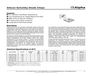
the anode. Electrical Specifications at 25C CJ1 (pF) RT2 ) ( VF @ 1 mA (mV) VB3 (V) RV @ Zero Bias ) (k Max. Max. Min.-Max. Min. Typ. 0.25 30 135-240 1 5.5 Part Number Barrier Junction Type CDC7630-000 ZBD P CDC7631-000 ZBD P 0.15 80 150-300 2 7.2 526-006 CDB7619-000 Low P 0.10 40 275-375 2 735 526-006 CDB7620-000 Low P 0.15 30 250-350 2 537 526-006 CDF7621-000 Low N 0.10 20 270-350 2 680 526-011 CDF7623-000 Low N 0.30 10 240-300 2 245 526-011 Outline Drawing 526-006 1. CJ for low barrier diodes specified at 0 V. CJ for ZBDs specified at 0.15 V reverse bias. 2. RT is the slope resistance at 10 mA. RS Max. may be calculated from: RS = RT - 2.6 x N. 3. VB for low barrier diodes is specified at 10 A. VB for ZBDs is specified at 100 A. Alpha Industries, Inc. [781] 935-5150 * Fax [617] 824-4579 * Email sales@alphaind.com * www.alphaind.com Specifications subject to change without notice. 8/01A 1 Silicon Schottky Diode Chips Typical Performance Data Detected Voltage (mV) 10000 DETECTOR VOLTAGE RF SOURC
 3 Pages, 294 KB, Original