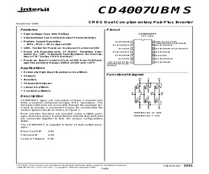
CD4007UBMS CMOS Dual Complementary Pair Plus Inverter November 1994 Features Pinout * High-Voltage Type (20V Rating) CD4007UBMS TOP VIEW * Standardized Symmetrical Output Characteristics * Medium Speed Operation - tPHL, tPLH = 30 ns (typ) at 10V Q2 (P) DRAIN 1 14 VDD, Q1, Q2, Q3 (P) SUBSTRATES, Q1(P) DRAIN Q2 (P) SOURCE 2 * 100% Tested for Maximum Quiescent Current at 20V 13 Q1 (P) SOURCE Q2 GATES 3 * Meets All Requirements of JEDEC Tentative Standards No. 13B, "Standard Specifications for Description of "B" Series CMOS Devices" 12 Q3 (N) DRAIN, Q3 (P) SOURCE Q2 (N) SOURCE 4 11 Q3 (P) DRAIN Q2 (N) DRAIN 5 10 Q3 GATES Q1 GATES 6 * Maximum Input Current of 1A at 18V Over Full Package-Temperature Range; 100nA at 18V and +25oC VSS, Q1, Q2, Q3 (N) SUBSTRATES Q1 (N) SOURCE 9 Q3 (N) SOURCE 8 Q1 (N) DRAIN 7 Applications * Extremely High-Input Impedance Amplifiers Functional Diagram * Shapers 14 * Inverters * Threshold Detector p 2 11 p p * Linear Amplifiers * Crystal Oscillators 6 13 Descrip
 9 Pages, 85 KB, Original
CD4007UBMS S E M I C O N D U C T O R CMOS Dual Complementary Pair Plus Inverter November 1994 Features Pinout * High-Voltage Type (20V Rating) CD4007UBMS TOP VIEW * Standardized Symmetrical Output Characteristics * Medium Speed Operation - tPHL, tPLH = 30 ns (typ) at 10V Q2 (P) DRAIN 1 14 VDD, Q1, Q2, Q3 (P) SUBSTRATES, Q1(P) DRAIN Q2 (P) SOURCE 2 * 100% Tested for Maximum Quiescent Current at 20V 13 Q1 (P) SOURCE Q2 GATES 3 * Meets All Requirements of JEDEC Tentative Standards No. 13B, "Standard Specifications for Description of "B" Series CMOS Devices" 12 Q3 (N) DRAIN, Q3 (P) SOURCE Q2 (N) SOURCE 4 11 Q3 (P) DRAIN Q2 (N) DRAIN 5 10 Q3 GATES Q1 GATES 6 * Maximum Input Current of 1A at 18V Over Full Package-Temperature Range; 100nA at 18V and +25oC VSS, Q1, Q2, Q3 (N) SUBSTRATES Q1 (N) SOURCE 9 Q3 (N) SOURCE 8 Q1 (N) DRAIN 7 Applications * Extremely High-Input Impedance Amplifiers Functional Diagram * Shapers 14 * Inverters * Threshold Detector p 2 11 p p * Linear Amplifiers * Crysta
 9 Pages, 79 KB, Original
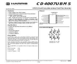
CD4007UBMS CMOS Dual Complementary Pair Plus Inverter November 1994 Features Pinout * High-Voltage Type (20V Rating) CD4007UBMS TOP VIEW + Standardized Symmetrical Output Characteristics Ad + Medium Speed Operation @2 (P) DRAIN [71] 4] VDD, @1, G2, Gs (P) SUBSTRATES, @1(P) DRAIN - tPHL, tPLH = 30 ns (typ) at 10V Q2 (P) SOURCE E 3] Q1 (P) SOURCE 100% Tested for Maximum Quiescent Current at 20V Q2 GATES EI 2] Qs (N) DRAIN, Qs (P} SOURCE Meets All Requirements of JEDEC Tentative Stan- Q2 (N} SOURCE 4 | Qs (P) DRAIN dards No. 13B, Standard Specifications for Descrip- tion of B Series CMOS Devices 02 (N) DRAIN EI ia) OS GATES . Qi GATES Ee 3] Qs (N) SOURCE Maximum Input Current of 1A at 18V Over Full Pack- age-Temperature Range; 100nA at 18V and +25C cupeTMaTee ot iN) GE [3] 21 (N) DRAIN SOURCE Applications + Extremely High-Input Impedance Amplifiers + Shapers Functional Diagram Inverters Threshold Detector + Linear Amplifiers + Crystal Oscillators Description CD4007BMS types are comprise
 9 Pages, 213 KB, Scan
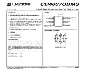
CD4007UBMS CMOS Dual Complementary Pair Plus Inverter November 1994 Features Pinout * High-Voltage Type (20V Rating) CD4007UBMS TOP VIEW * Standardized Symmetrical Output Characteristics * Medium Speed Operation - tPHL, tPLH = 30 ns (typ) at 10V Q2 (P) DRAIN 1 14 VDD, Q1, Q2, Q3 (P) SUBSTRATES, Q1(P) DRAIN Q2 (P) SOURCE 2 * 100% Tested for Maximum Quiescent Current at 20V 13 Q1 (P) SOURCE Q2 GATES 3 * Meets All Requirements of JEDEC Tentative Standards No. 13B, "Standard Specifications for Description of "B" Series CMOS Devices" 12 Q3 (N) DRAIN, Q3 (P) SOURCE Q2 (N) SOURCE 4 11 Q3 (P) DRAIN Q2 (N) DRAIN 5 10 Q3 GATES Q1 GATES 6 * Maximum Input Current of 1A at 18V Over Full Package-Temperature Range; 100nA at 18V and +25oC VSS, Q1, Q2, Q3 (N) SUBSTRATES Q1 (N) SOURCE 9 Q3 (N) SOURCE 8 Q1 (N) DRAIN 7 Applications * Extremely High-Input Impedance Amplifiers Functional Diagram * Shapers 14 * Inverters * Threshold Detector p 2 11 p p * Linear Amplifiers * Crystal Oscillators 6 13 Descrip
 9 Pages, 85 KB, Original
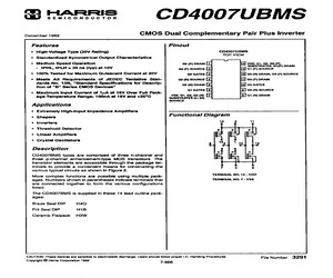
CD4007UBMS TH3-2Q] CMOS Dual Complementary Pair Plus Inverter December 1992 Features Pinout * High-Voltage Type (20V Rating) oe epsso7uEMs * Standardized Symmetrical Output Characteristics , Medium Speed Operation , @2 (Py DRAIN [7 Ha] VOD, a1, G2, 03 (P : BSTRATES, Q1(P) DRAIN + tPHL, tPLH = 30 ns (typ) at 10V - @2@ysounce [2] Hs] 01 (F) SOURCE * 100% Tested for Maximum Quiscent Current at 20V ~ a 02 Gates Bl H12] @3 (N} DRAIN, G3 (P) SOURCE Meets All Requirements of JEDEC Tentative Stan- |. a2 (ny source [4] 11] G3 (P) DRAIN dards No. 138, Standard Specifications for Descrip- . tlon of B Serles CMOS Devices a2 om prawn [s fol as cares a1 cares [6] [9] 03 (N) SOURCE Maximum Input Current of 1A at 18V Over Full Pack- | _ : : - age-Temperature Range; 100nA at 18V and +25C oer " [SJ Qt (N) DRAIN SOURCE Applications Extremely High-input Impedance Amplifiers 7 Shapers Functional Diagram * Inverters * Threshold Detector Linear Amplifiers * Crystal Oscillators Description CD4007BMS types are comprised
 9 Pages, 604 KB, Scan
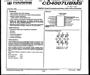
CD4007UBMS December 1992 CMOS Dual Complementary Pair Plus Inverter Features Pinout * High-Voltage Type (20V Rating) coao7UBMS iP * Standardized Symmetrical Output Characteristics * Medium Speed Operation " @2 (P) DRAIN [1 H14] VOD, @1, 22, G3 (P) SUBSTRATES, Q1(P) DRAIN ~ IPHL, tPLH = 30 ns (typ) at 10V a2(P) source [2 H3] at (P) SOURCE 100% Tested for Maximum Quiescent Current at 20V az cates [3 Ha] @3 (N) DRAIN, G3 (P) SOURCE Meets All Requirements of JEDEC Tentative Stan- a2 (ny source [4] 114] 3 (P) DRAIN dards No. 13B, Standard Specifications for Descrip- - tlon of "B Serles CMOS Devices a2 onan [5 Hol as cares at cates [6] 9] 03 (N) SOURCE Maximum Input Current of 1A at 18V Over Full Pack- age-Temperature Range; 100nA at 18V and +25C suBeTAATeS of 4 fz [2] 21 (N) DRAIN SOURCE Applications * Extremely High-Input Impedance Amplifiers = * Shapers Functional Diagram Inverters Threshold Detector Linear Amplifiers Crystal Osclilators Description CD4007BMS types are comprised of three n-channel a
 9 Pages, 306 KB, Scan