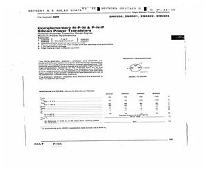
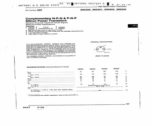
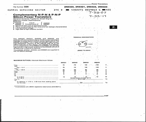
2N5320, 2N5321, 2N5322, 2N5323 Complementary N-P-N & P-N-P Silicon Power Transistors General-Purpose Types for Small-Signal, Medium-Power Applications Features: = 2N5322 P-N-P 2N5320 2N5323 Complements of: 2N5321 = Maximum safe-area-of-operation curves i = Planar construction for iow-noise and low leakage characteristics : = Low saturation voltage : = High beta at high collector current i | TERMINAL DESIGNATIONS | The RCA-2N5320, 2N5321, 2N5322 and 2N5323 are doubled-diffused epltaxial-planar silicon power transistors intended for small-signal medium-power applications. The 2N5320 and 2N5321 n-p-n types are actually high-current, high-dissipation versions of the 2N2102 with all of the | | salient features of that device. The 2N5322 and 2N5323, e (CASED p-n-p complements of the 2N5320 and 2N5321, are actually high-current, high-power versions of the 2N4036 with all of 92c$-27512 its additional outstanding features. ' The 2N5320, 2N53
 5 Pages, 232 KB, Scan
2N5320 2N5321 SMALL SIGNAL NPN TRANSISTORS SILICON EPITAXIAL PLANAR NPN TRANSISTORS MEDIUM POWER AMPLIFIER PNP COMPLEMENTS ARE 2N5322 AND 2N5323 DESCRIPTION The 2N5320 and 2N5321 are silicon epitaxial planar NPN transistors in Jedec TO-39 metal case. They are especially intended for high-voltage medium power application in industrial and commercial equipments. The complementary PNP types are respectively the 2N5322 and 2N5323 TO-39 INTERNAL SCHEMATIC DIAGRAM ABSOLUTE MAXIMUM RATINGS Symbol Parameter Value Uni t 2N5320 2N5321 V CBO Collector-Base Voltage (IE = 0) 100 75 V V CEV Collector-Emitter Voltage (V BE = 1.5V) 100 75 V V CEO Collector-Emitter Voltage (I B = 0) 75 50 V V EBO Emitter-Base Voltage (I C = 0) 6 5 IC I CM IB Collector Current A Collector Peak Current 2 A Base Current 1 A o P t ot Total Dissipation at T amb = 25 C P t ot Total Dissipation at T c = 25 C T stg, T j June 1997 V 1.2 o Storage and Junction Temperature 1 W 10 W -65 to 200 o C 1/4 2N5320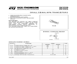 4 Pages, 34 KB, Original
4 Pages, 34 KB, Original2N5320 2N5321 SMALL SIGNAL NPN TRANSISTORS SILICON EPITAXIAL PLANAR NPN TRANSISTORS MEDIUM POWER AMPLIFIER PNP COMPLEMENTS ARE 2N5322 AND 2N5323 DESCRIPTION The 2N5320 and 2N5321 are silicon epitaxial planar NPN transistors in Jedec TO-39 metal case. They are especially intended for high-voltage medium power application in industrial and commercial equipments. The complementary PNP types are respectively the 2N5322 and 2N5323 TO-39 INTERNAL SCHEMATIC DIAGRAM ABSOLUTE MAXIMUM RATINGS Symbol Parameter Value 2N5320 Unit 2N5321 V CBO Collector-Base Voltage (I E = 0) 100 75 V V CEV Collector-Emitter Voltage (V BE = 1.5V) 100 75 V V CEO Collector-Emitter Voltage (I B = 0) 75 50 V V EBO Emitter-Base Voltage (I C = 0) 6 5 IC I CM IB Collector Current A Collector Peak Current 2 A Base Current 1 A o P tot Total Dissipation at T amb = 25 C P tot Total Dissipation at T c = 25 o C T stg , T j June 1997 V 1.2 Storage and Junction Temperature 1 W 10 W -65 to 200 o C 1/4 2N5320 4 Pages, 45 KB, Original
4 Pages, 45 KB, Original! Sy 110A 200C | 50WC 30M sooP | 30/90 BA AHs | OBS | 2N5290 2N5319 NS | TO61 | Leo | 100v | 1o0vV! bv | 10A 200C | 50WwC 30M BOOP | 30/90 5A AHS | 08S | 2N5288 2NS5320 NS | TO39 | Loa j100v | ev | 7v [2A 200C | 1WF 50M : 30/130 | 500mA | AMH| RCA | BSS42 2N5320 2N5320-R NS | TOS | Lod | 100v | Jev | 7 [24a 200C | 10WC 50M 20P | 33/50 s00mA | RMS | FCD | BSS15 2N2102 2N5320-BR NS [TOS j Los ; 100V ; 7EV 7 TV [2A 200C } 10WC 50M 20P | 25/38 s00mA | RMS] FCD | BSS15 2N2102 2N5320-0 NS | TOS | Loa | 100v | 75v Tv} 2A 200C | 10WC 50M 20P | 43/65 500mA | RMS | FCD | BSS15 2N2102 2N5320-Y Ns | Tos | to4 | 100v | 7ev | 7 [2A 200C | 10wc 50M 20P | 56/85 s00mA | RMS} FCD | BSS15 2N2102 2N5320-GN | NS | TOS | Los | 100v; 75v | JV /2A 200c | 10WC 50M 20P j 73/100 | 500mA | RMS | FCD | BSS15 2N2102 2N5320-BL NS | Tos | Loa | 100v | 7ev | 7v [2A 200C | 10WC 50M 20P | 95/145 | 500mA | RMS| FCD | BSS15 2N2102 2N5320-V NS
 1 Pages, 85 KB, Scan
2N5320, 2N5321, 2N5322, 2N5323 Complementary N-P-N & P-N-P Silicon Power Transistors General-Purpose Types for Small-Signal, Medium-Power Applications Features: = 2N5322 P-N-P 2N5320 2N5323 Complements of: 2N5321 Maximum safe-area-of-operation curves i Planar construction for low-noise and low leakage characteristics : Low saturation voltage ' High beta at high collector current i TERMINAL DESIGNATIONS The RCA-2N5320, 2N5321, 2N5322 and 2N5323 are doubled-diffused epitaxial-planar silicon power transistors intended for small-signal medium-power applications. The 2N5320 and 2N5321 n-p-n types are actually high-current, high-dissipation versions of the 2N2102 with all of the salient features of that device. The 2N5322 and 2N5323, E (CASE) | p-n-p complements of the 2N5320 and 2N5321, are actually high-current, high-power versions of the 2N4036 with all of 9208-27512 its additional outstanding features. i The 2N5320, 2N5321, 2N5322, an
 5 Pages, 361 KB, Scan
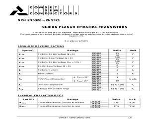
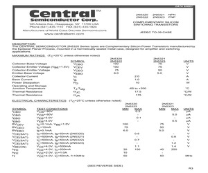
2N5320 2N5321 MEDIUM-POWER AMPLIFIERS DESCRIPTION The 2N5320 and 2N5321 are silicon planar epitaxial NPN transistors in Jedec TO-39 metal case. They are especially intended for high-voltage medium power applications in industrial and commercial equipments. The complementary PNP types are respectively the 2N5322 and 2N5323. TO-39 INTERNAL SCHEMATIC DIAGRAM ABSOLUTE MAXIMUM RATINGS Symbol Parameter Value 2N 5320 2 N 5321 Unit V CBO Collector-base Voltage (I E = 0) 100 75 V V CEV Collector-emitter Voltage (V BE = 1.5 V) 100 75 V V CEO Collector-emitter Voltage (I B = 0) 75 50 V V EBO Emitter-base Voltage (I C = 0) 6 5 V IC Collector Current 2 IB Base Current 1 A Total Power Dissipation at T amb 25 C at T c ase 25 C 1 10 W W - 65 to 200 C Pt o t T s t g, T j October 1988 Storage and Junction Temperature A 1/4 2N5320-2N5321 THERMAL DATA R t h j- cas e R t h j-amb Thermal Resistance Junction-case Thermal Resistance Junction-ambient Max Max C/W C/W 17.5 175 ELECTRICAL CHARACTER
 4 Pages, 51 KB, Original
2N5320, 2N5321, 2N5322, 2N5323 HARRIS SEMICOND SECTOR Cee Dd = uadee sh GOu5aES b MEHAS Cc | t N-P-N & P-N-P 1338-07 omplementary N-P- -N- Silicon Power Transistors w 1 O57 1 General-Purpose Types for Small-Signal, Medium-Power Applications Features: = 2N5322 P-N-P 2N5320 2N5323 Complements of: 2N5321 Maximum safe-area-of-operation curves Planar construction for low-noise and low leakage characteristics , a. Low saturation voltage - some ca High beta at high collector current - TERMINAL DESIGNATIONS The 2N5320, 2N5321, 2N5322 and 2N5323 are doubled-diffused epitaxial-planar silicon power transistors intended for small-signal medium-power applications. The 8 2N5320 and 2N5321 n-p-n types are actually high-current, . high-dissipation versions of the 2N2102 with ail of the salient features of that device. The 2N5322 and 2N5323, E CICASED p-n-p complements of the 2N5320 and 2N5321, are actually . . . high-current, high-power versions of the 2N4036 w
 5 Pages, 387 KB, Scan
2N5320 - 2N5321 SILICON PLANAR EPITAXIAL TRANSISTORS The 2N5320 and 2N5321 are NPN transistors mounted in TO-39 metal case . They are especially intended for high-voltage medium power applications in industrial and commercial equipements. Compliance to RoHS ABSOLUTE MAXIMUM RATINGS Symbol Ratings VCEO Collector-Emitter Voltage (IB = 0) VCBO Collector-Base Voltage (IE = 0) VCEV Collector-Emitter Voltage (VBE = 1.5V) VEBO Emitter-Base Voltage (IC = 0) IC Collector Current IB Base Current PD Total Power Dissipation @ Tamb = 25 @ Tcase= 25 TJ Junction Temperature TStg Storage Temperature range Value 2N5320 2N5321 2N5320 2N5321 2N5320 2N5321 2N5320 2N5321 2N5320 2N5321 2N5320 2N5321 2N5320 2N5321 2N5320 2N5321 2N5320 2N5321 2N5320 2N5321 Unit 75 50 100 75 100 75 6 5 V V V V 2 A 1 A 1 Watts 10 -65 to +200 C -65 to +200 C THERMAL CHARACTERISTICS Symbol Ratings Rt
 3 Pages, 181 KB, Original
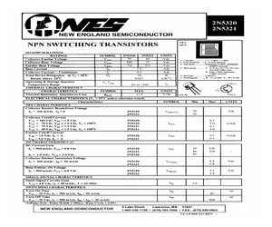
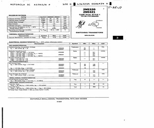
2N5320 = PACER PAT ug B FNEW ENGLAND SEMICONDUCTOR NPN NPN SWITCHING TRANSISTORS 1075 MAXIMUM RATINGS RATINGS SYMBOL 2N5320 | 2N5321 UNITS Collector-Emitter Voltage Veo 75 50 Vdc 1, Chip size 78475 mils + 2mils Collector-Base Voltage Vso 100 75, Vde 2. Chip thickness.......8 - 12 mils nominal - 3. Top metal... Aluminum 25,000A minimum, Emitter-Base Voltage Vero 7.0 5.0 Vdc 30,000A nominal Base Current I; 1.0 Adc 4. Back metal............... A. Nig AK THA min., Collector Current -- Continuous Ic 2.0 Adc B. Gold 1,500A minimum, Total Device Dissipation @ 1. = 25C Pp 10 W , BachsidecrsenmnCollector Derate Above 25C 0.057 mW?C 6. Bonding pad... B= 19x8 mils, E=35 8 mils Operating & Storage Junction Temperature Range Th Tstg -65 to +200 ve 3 Collector THERMAL CHARACTERISTICS > CHARACTERISTICS SYMBOL MAX. UNITS Base Thermal Resistance, Junction-to-Case Rec 17.5 C/W TO39 1 Emitter ELECTRICAL CHARACTERISTICS (T, = 25 C unless otherwise noted) | Characteristics | SYMBOL | Min [| Max | UNITS |
 1 Pages, 50 KB, Scan
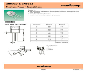
2N5320 & 2N5322 Medium Power Transistors Features: * High performance, low frequency devices typically with current ratings 2A. Up to 1W power dissipation. * Silicon Power Switching Transistors. * Medium Power Amplifier and Switching Applications. 2N5320 NPN 2N5322 PNP TO-39 Metal Can Package Dimensions Minimum Maximum A 8.50 9.39 B 7.74 8.50 C 6.09 6.60 D 0.40 0.53 E - 0.88 F 2.41 2.66 G 4.82 5.33 H 0.71 0.86 J 0.73 1.02 K 12.70 - L 42 48 Dimensions : Millimetres Pin Configuration 1. Emitter 2. Base 3. Collector Page 1 31/05/05 V1.0 2N5320 & 2N5322 Medium Power Transistors Absolute Maximum Ratings Description 2N5320 NPN 2N5322 PNP Symbol Collector Emitter Voltage VCEO 75 Collector Base Voltage VCBO 100 Emitter Base Voltage VEBO 7 Collector Current-Continuous IC 2.0 Base Current IB 1.0 Power Dissipation at Ta = 25C Derate above 25C Power Dissipation at Tc = 25C Derate above 25C V A 1 5.71 PD Operating and Storage Junction Temperature Range Units W mW/C 10 57
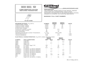
 4 Pages, 312 KB, Original
2N5320 2N5321 2N5322 2N5323 NPN PNP COMPLEMENTARY SILICON SWITCHING TRANSISTORS w w w. c e n t r a l s e m i . c o m DESCRIPTION: The CENTRAL SEMICONDUCTOR 2N5320, 2N5322 series types are complementary silicon power transistors manufactured by the epitaxial planar process, designed for amplifier and switching applications. MARKING: FULL PART NUMBER TO-39 CASE MAXIMUM RATINGS: (TC=25C) Collector-Base Voltage Collector-Emitter Voltage Collector-Emitter Voltage Emitter-Base Voltage Continuous Collector Current Continuous Base Current Power Dissipation Operating and Storage Junction Temperature Thermal Resistance Thermal Resistance SYMBOL VCBO VCEV VCEO VEBO IC IB PD TJ, Tstg JA JC 2N5320 2N5322 100 100 75 6.0 ELECTRICAL CHARACTERISTICS: (TC=25C unless otherwise noted) 2N5320 2N5322 SYMBOL TEST CONDITIONS MIN MAX ICBO VCB=80V 0.5 ICBO VCB=60V IEBO VEB=5.0V 0.1 IEBO VEB=4.0V BVCEV IC=100A, VBE=1.5V 100 BVCEO IC=10mA 75 BVEBO IE=100A 6.0 VCE(SAT) IC=500mA, IB=50mA
 3 Pages, 322 KB, Original
 1W 5W 1W 1W 0.8W 0.8W 0.8W 5W 6W 6W 6W 6W 0.8W 0.8W 0.8W 0.8W 5W 5W 1W 0.8W 0.8W 1W 1W 1W 2W 2W 2W 2W 2W 2W 2W 2W 2W 1W 1W PD 1W 2W 2W 2W 2W 2W 1W 10W 10W 2N5151S 2N5152 2N5152A 2N5152S 2N5153 2N5153S 2N5154 2N5154A 2N5154S 2N5154X 2N5154XX 2N5237 2N5238 2N5320 2N5320X 2N5322 2N5323 2N5333 2N5334 2N5335 2N5336 2N5336CECC 2N5336X 2N5337 2N5337CECC 2N5337X 2N5338 2N5338CECC 2N5338X 2N5339 2N5339CECC 2N5339X 2N5404 2N5405 2N5406 2N5407 2N5407L 2N5407X 2N5414 2N5414CECC 2N5415 PRODUCT 2N5415CECC 2N5416 2N5416CECC 2N5662 2N5663 2N5666 2N5667 2N5679 2N5681 2N5682 2N5781 2N5781XL 2N5782 2N5782L 2N5783 PNP NPN NPN NPN PNP PNP NPN NPN NPN NPN NPN NPN NPN NPN NPN PNP PNP PNP NPN NPN NPN NPN NPN NPN NPN NPN NPN NPN NPN NPN NPN NPN PNP PNP PNP PNP PNP PNP NPN NPN PNP Status Polarity PNP PNP PNP NPN NPN NPN NPN PNP NPN NPN PNP PNP PNP PNP PNP TO39 (TO205AD) TO39 (TO205AD) TO39 (TO205AD) TO39 (TO205AD) TO39 (TO205AD) TO39 (TO205AD) TO39 (TO205AD) TO39 (TO205AD) TO39 (TO205AD) TO39 (TO205AD) TO39
 1197 Pages, 40410 KB, Original
2N5320, 2N5322 Series Medium Power Bipolar Transistors Features: * High performance, low frequency devices typically with current ratings 1A. Up to 1W power dissipation. * Silicon power switching transistors. * Medium power amplifier and switching applications. TO-39 Metal Can Package Dimensions Minimum Maximum A 8.50 9.39 B 7.74 8.50 C 6.09 6.60 D 0.40 0.53 E - 0.88 F 2.41 2.66 G 4.82 5.33 H 0.71 0.86 J 0.73 1.02 K 12.70 - L 42 48 Dimensions : Millimetres Pin Configuration 1. Emitter 2. Base 3. Collector Page 1 15/03/06 V1.0 2N5320, 2N5322 Series Medium Power Bipolar Transistors Absolute Maximum Ratings Symbol 2N5320 2N5322 Collector Emitter Voltage VCEO 75 Collector Base Voltage VCBO 100 Emitter Base Voltage VEBO 7 Collector Current-Continuous IC 2.0 Base Current IB 1.0 Description Power Dissipation at Ta = 25C Derate Above 25C Power Dissipation at Tc = 25C Derate Above 25C PD Operating and Storage Junction Temperature Range Tj, Tstg -65 to +200 Junction to Ambient in
 4 Pages, 138 KB, Original
2N5320 2N5322 2N5321 2N5323 NPN PNP COMPLEMENTARY SILICON SWITCHING TRANSISTORS JEDEC TO-39 CASE DESCRIPTION The CENTRAL SEMICONDUCTOR 2N5320 Series types are Complementary Silicon Power Transistors manufactured by the Epitaxial Planar Process, mounted in a hermetically sealed metal case, designed for amplifier and switching applications. MAXIMUM RATINGS (TC=25C unless otherwise noted) SYMBOL Collector-Base Voltage VCBO Collector-Emitter Voltage (VBE=1.5V) VCEV Collector-Emitter Voltage VCEO Emitter-Base Voltage VEBO Collector Current IC Base Current IB Power Dissipation PD Operating and Storage Junction Temperature TJ,Tstg Thermal Resistance JC Thermal Resistance 2N5320 2N5322 100 100 75 6.0 2N5321 2N5323 75 75 50 5.0 2.0 1.0 10 JA UNITS V V V V A A W -65 to +200 C 17.5 C/W 175 C/W ELECTRICAL CHARACTERISTICS (TC=25C unless otherwise noted) SYMBOL ICBO ICBO IEBO IEBO BVCEV BVCEO BVEBO VCE(SAT) VCE(SAT) VCE(SAT) VCE(SAT) VBE(ON) hFE hFE fT TEST CONDITIONS VCB= 80V VCB= 60
 2 Pages, 108 KB, Original
2N5320 MAXIMUM RATINGS ee re. STYLE 1 Rating Symbol | 2N5320 | 2N5321| Unit -39 (TO-205AD) Collector-Emitter Voltage VcEO 75 50 Vde Collector-Base Voltage Vcs0 100 75 Vde 3 Collector Emitter-Base Voltage VEBO 7.0 5.0 Vde Base Current Ig 1.0 Ade 2 Collector Current Continuous Ic 2.0 Ade Base Total Device Dissipation @ Tc = 25C Pp 10 Watts 3 . Derate above 26C 0.057 mWwrc ani 1 Emitter Operating and Storage Junction Ty. Tstg 65 to +200 C Temperature Range SWITCHING TRANSISTORS THERMAL CHARACTERISTICS Characteristic Symbol Max Unit NPN SILICON Thermal Resistance, Junction to Case Rac 17,5 CW ELECTRICAL CHARACTERISTICS (Ta = 25C unless otherwise noted.) / Characteristic | Symbol | Min L Max Unit OFF CHARACTERISTICS Collector-Emitter Breakdown Voltage V(gR)CEO Vde (ig = 100 mAdg, Ip = 0} 2N5320 75 _ 2N5321 50 Collector Cutoff Current IcEx mAdc (Vce = 100 Vde, Vee = 1.5 Vdc) 2N5320 ~ 0.1 (Vce = 70 Vdc, Vge = 1.5 Vde, Te = 160C) =- 5.0 (Vce = 76 Vde, Vag = 1.5 Vde)
 2 Pages, 120 KB, Scan