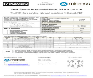
2N4117A N-CHANNEL JFET Linear Systems replaces discontinued Siliconix 2N4117A The 2N4117A is an Ultra-High Input Impedance N-Channel JFET The 2N4117A provides ultra-high input impedance. The device is specified with a 1-pA limit and typically operates at 0.2 pA. The part is ideal for use as a highimpedance sensitive front-end amplifier. 2N4117A Benefits: Insignificant Signal Loss / Error Voltage with High-Impedance Source Low Power Consumption (Battery) Maximum Signal Output, Low Noise High Sensitivity to Low-Level Signals 2N4117A Applications: High-Impedance Transducer Smoke Detector Input Infrared Detector Amplifier Precision Test Equipment FEATURES DIRECT REPLACEMENT FOR SILICONIX 2N4117A LOW POWER MINIMUM CIRCUIT LOADING ABSOLUTE MAXIMUM RATINGS @ 25C (unless otherwise noted) Maximum Temperatures Storage Temperature Operating Junction Temperature Maximum Power Dissipation Continuous Power Dissipation MAXIMUM CURRENT
 1 Pages, 778 KB, Original
N4859 3-28 5-3 2N4092A N JFET 2N4092 2N4859A N JFET 2N4859A 3-29 5-3 2N4093 N JFET 2N4093 3-19 5-3 2N4859JAN N JFET 2N4859JAN 5-3 2N4093A N JFET 2N4093 2N485QJANTX N JFET 2N4859JANTX 5-3 2N4117 N JFET 2N4117 3-20 5-29 2N4859JANTXV NN JFET 2N4859JANTXV 5-3 2N4117A N JFET 2N4117A 3-20 -29 2N4860 N JFET 2N4860 3-28 5-3 2N4118 N JFET 2N4118 3-20 5-29 2N4860A N JFET 2N4860A 3-29 5-3 2N4118A N JFET 2N4118A 3-20 -29 2N4860JAN N JFET 2N4860JAN 5-3 2N4119 N JFET 2N4119 3-20 5-29 2N4860JANTX = N JFET 2N4860JANTX -3 2N4119A N JFET 2N4119A 3-20 5-29 2N4860JANTXV N JFET 2N4860JANTXV 5-3 2N4120 P MOS ENH 3N163 2N4861 N JFET 2N4861 3-28 5-3 2N4139 N JFET 2N3822 2N4861A N JFET 2N4861A 3-29 5:3 2N4220 N JFET 2N4220 3-22 5-25 2N4861JAN N JFET 2N4861JAN 5-3 2N4220A N JFET 2N4220A 3-22 -25 2N4861JANTX = N JFET 2N4861JANTX 5-3 2N4221 N JFET 2N4221 3-22 5-25 2N4861JANTXV N JFET 2N4861JANTXV 5-3 2N4221A N JFET 2N4221A 3-22 5-25 2N4867 N JFET 2N4867 3-30 5-27 2N4222 N JFET 2N4222 3-22 5-25 2N4867A N JFET 2N
 268 Pages, 11688 KB, Scan
2N4117A N-CHANNEL JFET Linear Systems replaces discontinued Siliconix 2N4117A The 2N4117A is an Ultra-High Input Impedance N-Channel JFET The 2N4117A provides ultra-high input impedance. The device is specified with a 1-pA limit and typically operates at 0.2 pA. The part is ideal for use as a highimpedance sensitive front-end amplifier. 2N4117A Benefits: Insignificant Signal Loss / Error Voltage with High-Impedance Source Low Power Consumption (Battery) Maximum Signal Output, Low Noise High Sensitivity to Low-Level Signals 2N4117A Applications: High-Impedance Transducer Smoke Detector Input Infrared Detector Amplifier Precision Test Equipment FEATURES DIRECT REPLACEMENT FOR SILICONIX 2N4117A LOW POWER MINIMUM CIRCUIT LOADING ABSOLUTE MAXIMUM RATINGS @ 25C (unless otherwise noted) IDSS<90 A IGSS<1 pA Maximum Temperatures Storage Temperature Operating Junction Temperature Maximum Power Dissipation Continuous Power Dissipa
 1 Pages, 289 KB, Original
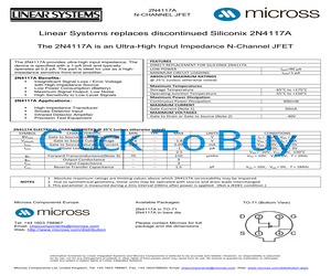
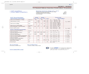
2N4117A SERIES N-Channel JFETs The 2N4117A Series are n-channel JFETs designed to provide ultra-high input impedance. The 2N4117A Series is specified with a 1 pA limit and typically operates at 0.2 pA. These devices, therefore, make perfect choices for use as sensitive front-end amplifiers in applications such as microphones, smoke detectors, and precision test equipment. Additionally, its hermetically sealed TO-72 package allows full military processing per MIL-S-19500. (See Section 1.) For additional design information please consult performance curves NT. SIMILAR PRODUCTS e TO-92, See PN4117A Series @ Duals, See U421 Series e Chips, See NT Series Die Vasvorn Viencss Ots Ipss PART M MIN MIN MAX NUMBER (V) (Vy) (uS) (mA) 2N4117A -18 -40 70 0.09 2N4118A -3 -40 80 0.24 2N4119A -6 ~40 100 0.60 TO-72 (TO-206AF) BOTTOM VIEW 1 SOURCE 2 DRAIN 3 GATE 4 CASE ABSOLUTE MAXIMUM RATINGS (Ta = 25C Unless Otherwise Noted) PARAMETERS/TEST CONDITIONS SYMBOL LIMITS UNITS Gat
 2 Pages, 47 KB, Scan
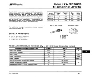
2N4117A 2N4118 2N4118A 2N4119 2N4119A iconix n-channel JFETs designed for. . +F Siliconix Performance Curves NT *JEDEC registered data. NOTES: e See Section 5 eo @ Ultra-High Input BENEFITS ege Impedance Amplifiers Low Power Ipss < 90 uA (2N4117) Electrometers @ Minimum Circuit Loading Tr I <1 pA (2N4117A Series) pH Meters GSS Smoke Detectors o TO-72 *ABSOLUTE MAXIMUM RATINGS (25C) See Section 7 Gate-Drain or Gate-Source Voltage (Note 1) ........ -40V Gate-Current ...... 0.0.0 cc cece cece ee eevee 50 mA Total Device Dissipation (Derate 2 mW/C to 175C) ..........00006e 300 mw Storage Temperature Range.............. -65 to +175C Lead Temperature (1/16 from case for 10 seconds).............. 255C s *ELECTRICAL CHARACTERISTICS (25C unless otherwise noted) 2N4117 2N4118 2N4119 Characteristic 2N4117A 2N4118A 2N4119A_} Unit Test Conditions Min | Max Min | Max | Min | Max i Gate Reverse Current -10 =10 ~10 | pA _ _ 2 5 'Gss 2N4117 Series Only -25 -25 -25 nA Vas = -20 V, Vps = 0
 4 Pages, 160 KB, Scan
N4858 2N4859 2N4859A 2N4860 2N4860A 2N4861 2N4861A 2N4867 2N4867A TEMIC Part Number 2N4340 2N4338 2N4338 2N4341 J177 2N4340 2N4341 2N4416 U401 U401 2N5196 2N5196 2N5197 2N5196 2N5199 2N5199 U401 U404 2N4391 2N4391 2N4392 2N4392 2N4393 2N4393 2N4391 2N4392 2N4117A 2N4118A 2N4119A 3N163 2N4340 2N4340 2N4341 2N4341 2N4341 2N4341 2N4416 2N4416 3N163 SST4416 2N5432 2N5433 2N5432 2N5432 2N4856A 2N4857A 2N4858A 2N4856A 2N4856A 2N4857A 2N4857A 2N4858A 2N4858A 2N4338 2N4338 Page 3 of 128 Approximate ReplacemenMfg SIL SIL SIL SIL SIL SIL SIL SIL SIL SIL SIL SIL SIL SIL SIL SIL SIL SIL SIL SIL SIL SIL SIL SIL SIL SIL SIL SIL SIL SIL SIL SIL SIL SIL SIL SIL SIL SIL SIL SIL SIL SIL SIL SIL SIL SIL SIL SIL SIL SIL SIL SIL SIL SIL SIL Industry Part Number 2N4868 2N4868A 2N4869 2N4869A 2N4977 2N4978 2N4979 2N5018 2N5019 2N5045 2N5046 2N5047 2N5104 2N5105 2N5245 2N5246 2N5247 2N5358 2N5361 2N5362 2N5363 2N5364 2N5398 2N5452 2N5453 2N5454 2N5456 2N5457 2N5458 2N5459 2N5459 2N5515 2N5516 2N5517 2N5518 2N5519 2N5520
 128 Pages, 241 KB, Original
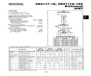
2N4117A-19A N-Channel JFET FEATURES PIN Low Leakage Iqgg <1 pA CONFIGURATION Low Capacitance C... << 1.5 pF p rss p 10-72 ABSOLUTE MAXIMUM RATINGS @ 25C (unless otherwise noted) Maximum Temperatures Storage Temperature -65C to +200C Operating Junction Temperature +200C Lead Temperature (Soldering, a c 8 10 sec time limit) 300C . wo CHIP Maximum Power Dissipation Device Dissipation @ Free Air Temperature 300 mW oo Y Ot: Linear Derating 1.7 mw/Pc | . tet, Fe Maximum Voltages & Current ASE tos * bos Vv Gate to Source Voltage -40V GS Vgp Gate to Drain Voltage -40 V a r e 0120 . 0180 Ig Gate Current 50 mA inves e nore source TS isoate roti | a7 0028 hy NOMS eu ORDERING INFORMATION TO-72 WAFER CHIP 2N4117 2N4117/W | 2N4117/D 2N4117A | 2N4117A/W |2N4117A/D 2N4118 2N4118/W 2N4118/D 2N4118A | 2N4118A/W | 2N4118A/D, 2N4119 2N4119/W 2N4119/D 2N4119A | 2N4119A/W | 2N4119A/D ELECTRICAL CHARACTERISTICS (25C unless otherwise noted) 2N4117 2N4118 2N4119 PARAMETER 2N41
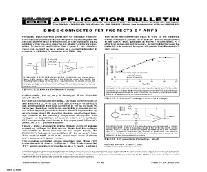
 1 Pages, 38 KB, Scan
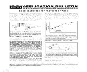
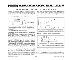
 must not degrade the op amp's performance. VDS = 0V 100 90 80 70 60 Thermal and Noise Threshold 10 0 5 10 15 20 25 VDG (V) JFET LEAKAGE CURRENTS can be so low that they don't degrade a lowinput bias op amp's parameters. Measurements show that Siliconix's 2N4117A can serve as a voltage limiter when it's diode-connected. The actual leakage is probably somewhat lower than measured, but thermal effects and noise place a limiting threshold on the measurement. FIGURE 1. Dielectric Evaluation Circuit. Unfortunately, the op amp is destroyed if the dielectric sample shorts. FIGURE 2. Curve of Leakage Current vs Voltage. For one such measurement setup, low-bias current op amps like the OPA111, OPA121, OPA128, OPA124 or OPA129 can serve because their bias current is in the pA or even fA range and therefore contributes negligible measurement error. What type of protective device doesn't degrade this op amp's parameters? PN-junction devices usually have leakage currents in the nanoamp range even at very-low
 3 Pages, 50 KB, Original
 must not degrade the op amp's performance. VDS = 0V 100 90 80 70 60 Thermal and Noise Threshold 10 0 5 10 15 20 25 VDG (V) JFET LEAKAGE CURRENTS can be so low that they don't degrade a lowinput bias op amp's parameters. Measurements show that Siliconix's 2N4117A can serve as a voltage limiter when it's diode-connected. The actual leakage is probably somewhat lower than measured, but thermal effects and noise place a limiting threshold on the measurement. FIGURE 1. Dielectric Evaluation Circuit. Unfortunately, the op amp is destroyed if the dielectric sample shorts. FIGURE 2. Curve of Leakage Current vs Voltage. For one such measurement setup, low-bias current op amps like the OPA111, OPA121, OPA128, OPA124 or OPA129 can serve because their bias current is in the pA or even fA range and therefore contributes negligible measurement error. What type of protective device doesn't degrade this op amp's parameters? PN-junction devices usually have leakage currents in the nanoamp range even at very-low
 2 Pages, 49 KB, Original
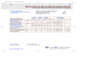
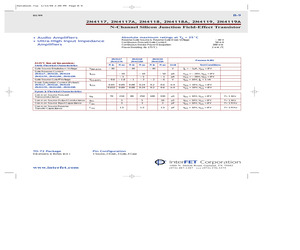
V f = 1 MHz 1000 N. Shiloh Road, Garland, TX 75042 (972) 487-1287 FAX (972) 276-3375 4 10 5 TO72 Package Pin Configuration Dimensions in Inches (mm) 1 Source, 2 Gate, 3 Drain, 4 Case www.interfet.com Databook.fxp 1/13/99 2:09 PM Page B-9 B-9 01/99 2N4117, 2N4117A, 2N4118, 2N4118A, 2N4119, 2N4119A N-Channel Silicon Junction Field-Effect Transistor Absolute maximum ratings at TA = 25C Audio Amplifiers Ultra-High Input Impedance Amplifiers Reverse Gate Source & Reverse Gate Drain Voltage Continuous Forward Gate Current Continuous Device Power Dissipation Power Derating (to 175C) 2N4117 2N4117A At 25C free air temperature: Static Electrical Characteristics Min Max - 40 2N4118 2N4118A Min Max Gate Source Breakdown Voltage V(BR)GSS - 40 Gate Reverse Current 2N4117, 2N4118, 2N4119 2N4117A, 2N4118A, 2N4119A IGSS Gate Source Cutoff Voltage VGS(OFF) - 0.6 - 1.8 -1 -3 Drain Saturation Current (Pulsed) 2N4117, 2N4118, 2N4119 2N4117A, 2N4118A, 2N4119A IGSS 0.03 0.09 0.08
 68 Pages, 1234 KB, Original
2N4117A, 2N4118, 2N4118A, 2N4119, 2N4119A N-Channel Silicon Junction Field-Effect Transistor Absolute maximum ratings at TA = 25C Audio Amplifiers Ultra-High Input Impedance Amplifiers Reverse Gate Source & Reverse Gate Drain Voltage Continuous Forward Gate Current Continuous Device Power Dissipation Power Derating (to 175C) 2N4117 2N4117A At 25C free air temperature: Static Electrical Characteristics Min Max - 40 2N4118 2N4118A Min Max Gate Source Breakdown Voltage V(BR)GSS - 40 Gate Reverse Current 2N4117, 2N4118, 2N4119 2N4117A, 2N4118A, 2N4119A IGSS Gate Source Cutoff Voltage VGS(OFF) - 0.6 - 1.8 -1 -3 Drain Saturation Current (Pulsed) 2N4117, 2N4118, 2N4119 2N4117A, 2N4118A, 2N4119A IGSS 0.03 0.09 0.08 0.015 0.09 70 210 2N4119 2N4119A Min Max - 40 - 40 V 50 mA 300 mW 2 mW/C Process NJ01 Unit Test Conditions V IG = - 1A, VDS = OV - 10 - 10 - 10 pA VGS = - 20V, VDS = OV -1 -1 -1 pA VGS = - 20V, VDS = OV -2 -6 V VDS = 10V, ID = 1 nA 0.24 0.2 0.6 mA VDS = 1
 1 Pages, 88 KB, Original
2N4117A, 2N4118, 2N4118A, 2N4119, 2N4119A N-Channel Silicon Junction Field-Effect Transistor Absolute maximum ratings at TA = 25C Audio Amplifiers Ultra-High Input Impedance Amplifiers Reverse Gate Source & Reverse Gate Drain Voltage Continuous Forward Gate Current Continuous Device Power Dissipation Power Derating (to 175C) 2N4117 2N4117A At 25C free air temperature: Static Electrical Characteristics Min Max - 40 2N4118 2N4118A Min Max Gate Source Breakdown Voltage V(BR)GSS - 40 Gate Reverse Current 2N4117, 2N4118, 2N4119 2N4117A, 2N4118A, 2N4119A IGSS Gate Source Cutoff Voltage VGS(OFF) - 0.6 - 1.8 -1 -3 Drain Saturation Current (Pulsed) 2N4117, 2N4118, 2N4119 2N4117A, 2N4118A, 2N4119A IGSS 0.03 0.09 0.08 0.015 0.09 70 210 2N4119 2N4119A Min Max - 40 - 40 V 50 mA 300 mW 2 mW/C Process NJ01 Unit Test Conditions V IG = - 1A, VDS = OV - 10 - 10 - 10 pA VGS = - 20V, VDS = OV -1 -1 -1 pA VGS = - 20V, VDS = OV -2 -6 V VDS = 10V, ID = 1 nA 0.24 0.2 0.6 mA VDS = 1
 17 Pages, 283 KB, Original
 must not degrade the op amp's performance. VDS = 0V 100 90 80 70 60 Thermal and Noise Threshold 10 0 5 10 15 20 25 VDG (V) JFET LEAKAGE CURRENTS can be so low that they don't degrade a lowinput bias op amp's parameters. Measurements show that Siliconix's 2N4117A can serve as a voltage limiter when it's diode-connected. The actual leakage is probably somewhat lower than measured, but thermal effects and noise place a limiting threshold on the measurement. FIGURE 1. Dielectric Evaluation Circuit. Unfortunately, the op amp is destroyed if the dielectric sample shorts. FIGURE 2. Curve of Leakage Current vs Voltage. For one such measurement setup, low-bias current op amps like the OPA111, OPA121, OPA128, OPA124 or OPA129 can serve because their bias current is in the pA or even fA range and therefore contributes negligible measurement error. What type of protective device doesn't degrade this op amp's parameters? PN-junction devices usually have leakage currents in the nanoamp range even at very-low
 1 Pages, 41 KB, Original
. 8V SO0yAmx 70/210pS : 3P0 1P5 | ALG | SLX | BFW13 2N3821 2N4117/D NJD | CHIP - 40V AmA | 200C - 0.6/1.8V SdpAmx 70/210pS - 3P0 1P5 | ALG | INS | BRW13 2N3821 2N4117WV NJD | SLICE 40V 1mA | 200 0.6/1.8V 90Amx 70/210pS - 3P0 1P5 | ALG | INS | BRW13 2N3821 2N4117A Nu | TO72 Ek 40v ImA | 200C] 300mWF 0.6/1.8 S0pAmx 70/210pS - 3P0 1P5 | ALG { SLX | BFW13 2N3821 2N4117A/0 NJO | CHIP . 40v 1mA | 200 - 0.6/1.8V S0pAmx 70/210uS . 3P0 1P5 | ALG | INS | BFW13 2N3821 2N4117AW NJD{ SLICE - 40v 1mA | 200 . 0.6/1.8V 90yAmx 70/210pS - 3P0 1P5 } ALG | INS | BFW13 2N3821 2N4117AT92 NJD | TO92 D 40V 1mA }125C] 300mWF 0.6/1.8V 90pAmx 70/210pS - 3P0 1P | ALG | INS | BF347 2N5457 2N4117CHP NJD | CHIP - 40V mA | 200 . 0.6/1.8V 30/100pA 70/210uS 3P0 1P5 } ALN | SLXy- 2N4117T092 NJD | TO92 DB 40v mA | 200C - 0.6/1.8V 90pAmx 70/210uS - 3P0 1P5 | ALG | INS | BF347 2N5457 2N4118 NJD | TO?72 tk 40V mA |200C} = 300mWF 13V 240pAmx 80/250pS 3P0 1P5 | ALG | SLX | BFW13 2N3821 2N4118/0 NJD
 1 Pages, 84 KB, Scan
We avmx 25mAmn : 60R 10P] 4P0 | RLS | SLX | BSV80 2N4392 2N5640 ND/ T1092. C |] 30Vi 250mA]135C] 310mWF 6vmx SmAmn -} 100R 10P] 4P0 | ALS | SLX | BSVa0 2N4393 2N5647 wuo| 1072 Ek | 50V] 2mA]150C] 300mwF 0.6/1.8V 300/600NA 300/650uS - 3P0) og | ALN | SLX]- 2N4117A 2N5648 NJO} 1072, Ek | SOV) 2ma]150c} 300mWF 0.8/2.4V 0.5/1mA 400/800pS : 3P0] OP9 ] ALN | SLX]- 2N4117A 2N5649 NID] To72. ek | SOV} =2mA|i150C| 300mwF 1V 0.8/1.6mA 450/900pS : 3P0} OPO | ALN | SLX]- 2N4117A 2N5653 ND} T0992. C | 30V] 200mA]150C] 310mwF 12Vmx 40mAmn : 50R 10P| 35 | RLS | TEL |ssv79 2N5653 2N565 Nuo| Tog2 sc | 30v| 150mA]150c] 3tomwe 12x 15mAmn -| 100k 10P| 3P5 | RLS | TEL }BSva0 2N4093 2ns668 WO} tos2 oc | 25vl sma|150c} 31omwr 0.2/4V +5mA imSmn : 7P0| 3P0 | RLG | TEL | BC264A 2NS457 2N5669 NiO} T0992. | (25v] toma] 150c] 310mwF vev 4/1omA 1.6mSmn . 7P0} 3P0 | RLG | TEL | BC264C 2N5458 2N5670 ND} 1092. GC f o2sv] 20mA4150C] atomwr 2/8V 8/20mA 2.5mSmn - 7P0{ 3P0 | ALG | TEL | BFWwet 2N5486 2N5716
 1 Pages, 90 KB, Scan