ssed RHA requirements. * 1.2 Package outlines. The device packages for the encapsulated device types are as follows: TO-39 and TO-5 in accordance with figure 1 1.3 Maximum ratings unless otherwise specified TA = +25C. Types 2N2218, 2N2219 2N2218A, 2N2219A 2N2218AL, 2N2219AL PT TA = +25C (1) W PT TC = +25C (1) W VCBO VCEO VEBO IC TSTG and TJ RJC max (2) RJA max (2) V dc V dc V dc mA dc For all C/W C/W 0.8 0.8 0.8 3.0 3.0 3.0 60 75 75 30 50 50 5 6 6 800 800 800 -65 to +200C 50 50 50 195 195 195 (1) See derating curve, figures 2 and 3. (2) For thermal impedance curves, see figures 4 and 5. * Comments, suggestions, or questions on this document should be addressed to DLA Land and Maritime, ATTN: VAC, P.O. Box 3990, Columbus, OH 43218-3990, or emailed to Semiconductor@dla.mil . Since contact information can change, you may want to verify the currency of this address information using the ASSIST Online database at https://assist.dla.mil . AMSC N/A FSC 5961 MIL-PRF-19500/251T 1.4 Primary electrical char
 26 Pages, 509 KB, Original
to comply with this document shall be completed by 12 August 2010. MIL-PRF-19500/251R 12 May 2010 SUPERSEDING MIL-PRF-19500/251P 7 April 2008 PERFORMANCE SPECIFICATION SHEET SEMICONDUCTOR DEVICE, TRANSISTOR, NPN, SILICON, SWITCHING, TYPES 2N2218, 2N2218A, 2N2218AL, 2N2219, 2N2219A, AND 2N2219AL, JAN, JANTX, JANTXV, JANS, JANSM, JANSD, JANSP, JANSL, JANSR, JANSF, JANSG, and JANSH This specification is approved for use by all Departments and Agencies of the Department of Defense. The requirements for acquiring the product described herein shall consist of this specification sheet and MIL-PRF-19500. 1. SCOPE 1.1 Scope. This specification covers the performance requirements for NPN, silicon, switching transistors. Four levels of product assurance are provided for each device type as specified in MIL-PRF-19500. RHA level designators "M", "D", "P", "L", "R", "F", "G", and "H" are appended to the device prefix to identify devices, which have passed RHA requirements. 1.2 Physical dimensions. See figure 1
 25 Pages, 299 KB, Original
2060 2N2060 2N2060 270 JANTXV2N2060 JANTXV2N2060 251 JAN2N2218 JAN2N2218 251 2N2218 2N2218 JANTX2N2218 JANTX2N2218 251 JANTXV2N2218 JANTXV2N2218 251 JAN2N2218A JAN2N2218A 251 2N2218A JANTX2N2218A 2N2218A JANTX2N2218A 251 JANTXV2N2218A JANTXV2N2218A 251 JAN2N2218ALJAN2N2218AL 251 2N2218AL JANTX2N2218AL 2N2218AL JANTX2N2218AL 251 JANTXV2N2218AL JANTXV2N2218AL 251 JAN2N2219 JAN2N2219 251 JANTX2N2219JANTX2N2219 251 2N2219 2N2219 JANTXV2N2219 JANTXV2N2219 251 JANS2N2219 JANS2N2219 251 JANSR2N2219JANSR2N2219 251 JAN2N2219A JAN2N2219A 251 JANTX2N2219A JANTX2N2219A 2N2219A 2N2219A 251 JANTXV2N2219A JANTXV2N2219A 251 JANS2N2219AJANS2N2219A 251 JANSR2N2219A JANSR2N2219A 251 JAN2N2219ALJAN2N2219AL 251 JANTX2N2219AL JANTX2N2219AL 251 2N2219AL JANTXV2219AL 2N2219AL JANTXV2219AL 251 JANS2N2219AL JANS2N2219AL 251 JANSR2N2219AL JANSR2N2219AL 255 JAN2N2222A JAN2N2222A 255 JANTX2N2222A JANTX2N2222A 255 2N2222A JANTXV2N2222A
 17 Pages, 6924 KB, Original
ssed RHA requirements. * 1.2 Package outlines. The device packages for the encapsulated device types are as follows: TO-39 and TO-5 in accordance with figure 1 1.3 Maximum ratings unless otherwise specified TA = +25C. Types 2N2218, 2N2219 2N2218A, 2N2219A 2N2218AL, 2N2219AL PT TA = +25C (1) W PT TC = +25C (1) W VCBO VCEO VEBO IC TSTG and TJ RJC max (2) RJA max (2) V dc V dc V dc mA dc For all C/W C/W 0.8 0.8 0.8 3.0 3.0 3.0 60 75 75 30 50 50 5 6 6 800 800 800 -65 to +200C 50 50 50 195 195 195 (1) See derating curve, figures 2 and 3. (2) For thermal impedance curves, see figures 4 and 5. * Comments, suggestions, or questions on this document should be addressed to DLA Land and Maritime, ATTN: VAC, P.O. Box 3990, Columbus, OH 43218-3990, or emailed to Semiconductor@dla.mil . Since contact information can change, you may want to verify the currency of this address information using the ASSIST Online database at https://assist.dla.mil . AMSC N/A FSC 5961 MIL-PRF-19500/251T 1.4 Primary electrical char
 26 Pages, 490 KB, Original
2N2218AL Qualified Level JAN JANTX JANTXV JANS 2N2219 2N2219A 2N2219AL MAXIMUM RATINGS Ratings Symbol Collector-Emitter Voltage Collector-Base Voltage Emitter-Base Voltage Collector Current Total Power Dissipation @ TA = +250C(1) @ TC = +250C(2) Operating & Storage Junction Temp. Range VCEO VCBO VEBO IC 2N2218 2N2219 2N2218A; L 2N2219A; L 30 60 5.0 50 75 6.0 PT Top, Tstg 800 0.8 3.0 -55 to +200 Unit Vdc Vdc Vdc mAdc W W 0 C TO- 39* (TO-205AD) 2N2218, 2N2218A 2N2219, 2N2219A THERMAL CHARACTERISTICS Characteristics Symbol Thermal Resistance, Junction-to-Case RJC 1) Derate linearly 4.6 mW/0C above TA > +250C 2) Derate linearly 17.0 mW/0C above TC > +250C Max. 59 Unit C/W 0 TO-5* 2N2218AL, 2N2219AL *See appendix A for package outline ELECTRICAL CHARACTERISTICS (TA = 250C unless otherwise noted) Characteristics Symbol Min. V(BR)CEO 30 50 Max. Unit OFF CHARACTERISTICS Collector-Emitter Breakdown Voltage IE = 10 mAdc Emitter-Base Cutoff Current VEB = 5.0 Vdc VEB = 6.0 Vdc VEB = 4.0 Vdc Coll
 10 Pages, 177 KB, Original
 0 C 2N2218, 2N2218A 2N2219, 2N2219A TO- 39 (TO-205AD) THERMAL CHARACTERISTICS Characteristics Thermal Resistance, Junction-to-Case 0 Symbol 0 RJC Max. 59 Unit C/mW 0 1) Derate linearly 4.6 mW/ C for TA > +25 C 2) Derate linearly 17.0 mW/0C for TC > +250C 2N2218AL, 2N2219AL TO-5 ELECTRICAL CHARACTERISTICS Characteristics Symbol Min. Max. Unit 2N2218, 2N2219 2N2218A, AL, 2N2219A, V(BR)CEO 30 50 2N2218, 2N2219 2N2218A, AL, 2N2219A, IEBO 10 10 10 Adc Adc ICES 10 10 Adc OFF CHARACTERISTICS Collector-Emitter Breakdown Voltage IE = 10 mAdc AL Emitter-Base Cutoff Current VEB = 5.0 Vdc VEB = 6.0 Vdc AL VEB = 4.0 Vdc Collector-Base Cutoff Current VCE = 30 Vdc VCE = 50 Vdc AL Vdc All Types 2N2218, 2N2219 2N2218A, AL, 2N2219A, 6 Lake Street, Lawrence, MA 01841 1-800-446-1158 / (978) 794-1666 / Fax: (978) 689-0803 Page 1 of 2 2N2218, A, AL; 2N2219, A, AL JAN SERIES ELECTRICAL CHARACTERISTICS (con't) Characteristics Collector-Base Cutoff Current VCB = 50 Vdc 2N2218, 2N2219 2N2218A, AL, 2N2219A, VCB = 60 Vdc A
 2 Pages, 31 KB, Original
2N2218AL Qualified Level JAN JANTX JANTXV JANS 2N2219 2N2219A 2N2219AL MAXIMUM RATINGS Ratings Symbol Collector-Emitter Voltage Collector-Base Voltage Emitter-Base Voltage Collector Current Total Power Dissipation @ TA = +250C(1) @ TC = +250C(2) Operating & Storage Junction Temp. Range VCEO VCBO VEBO IC 2N2218 2N2219 2N2218A; L 2N2219A; L 30 60 5.0 50 75 6.0 PT Top, Tstg 800 0.8 3.0 -55 to +200 Unit Vdc Vdc Vdc mAdc W W 0 C TO- 39* (TO-205AD) 2N2218, 2N2218A 2N2219, 2N2219A THERMAL CHARACTERISTICS Characteristics Symbol Thermal Resistance, Junction-to-Case RJC 1) Derate linearly 4.6 mW/0C above TA > +250C 2) Derate linearly 17.0 mW/0C above TC > +250C Max. 59 Unit C/W 0 TO-5* 2N2218AL, 2N2219AL *See appendix A for package outline ELECTRICAL CHARACTERISTICS (TA = 250C unless otherwise noted) Characteristics Symbol Min. V(BR)CEO 30 50 Max. Unit OFF CHARACTERISTICS Collector-Emitter Breakdown Voltage IE = 10 mAdc Emitter-Base Cutoff Current VEB = 5.0 Vdc VEB = 6.0 Vdc VEB = 4.0 Vdc Coll
 2 Pages, 49 KB, Original
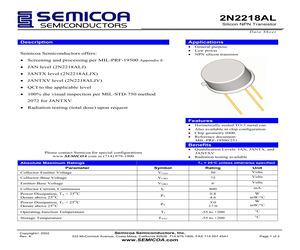
2N2218AL Silicon NPN Transistor Data Sheet Description Applications Semicoa Corporation offers: * General purpose * Low power * NPN silicon transistor * Screening and processing per MIL-PRF-19500 Appendix E * JAN level (2N2218ALJ) * JANTX level (2N2218ALJX) * JANTXV level (2N2218ALJV) * QCI to the applicable level * 100% die visual inspection per MIL-STD-750 method 2072 for JANTXV * Radiation testing (total dose) upon request Features * * * * Hermetically sealed TO-5 metal can Also available in chip configuration Chip geometry 0400 Reference document: MIL-PRF-19500/251 Benefits * Qualification Levels: JAN, JANTX, and JANTXV * Radiation testing available Please contact Semicoa for special configurations www.SEMICOA.com or (714) 979-1900 Absolute Maximum Ratings Parameter Collector-Emitter Voltage TC = 25C unless otherwise specified Symbol VCEO Rating 50 Collector-Base Voltage VCBO 75 Unit Volts Volts Emitter-Base Voltage VEBO 6 Volts Collector Current, Contin
 2 Pages, 440 KB, Original
2N2218AL JAN, JTX, JTXV 2N2219, 2N2219A JAN, JTX, JTXV 2N2219AL JAN, JTX, JTXV MIL-PRF QPL DEVICES Processed per MIL-PRF-19500/251 NPN SWITCHING SILICON TRANSISTOR MAXIMUM RATINGS Ratings Collector-Emitter Voltage Collector-Base Voltage Emitter-Base Voltage Collector Current Total Power Dissipation @ TA = +250C(1) @ TC = +250C(2) Operating & Storage Junction Temperature Range Symbol 2N2218 2N2219 2N2218A; L 2N2219A; L Unit VCEO VCBO VEBO IC PT 30 60 5.0 50 75 6.0 800 Vdc Vdc Vdc mAdc 0.8 3.0 -65 to +200 W W 0 C TJ, Tstg 2N2218, 2N2218A 2N2219, 2N2219A TO- 39 (TO-205AD) THERMAL CHARACTERISTICS Characteristics Symbol Thermal Resistance, RJC Junction-to-Case 0 1) Derate linearly 4.6 mW/ C for TA > +250C 2) Derate linearly 17.0 mW/0C for TC > +250C Max. 0.059 Unit C/mW 0 2N2218AL, 2N2219AL TO-5 ELECTRICAL CHARACTERISTICS (TA = 250C unless otherwise noted) Characteristics Symbol Min. Max. Unit 2N2218, 2N2219 2N2218A, L, 2N2219A, L V(BR)CBO 60 75 Vdc 2N2218, 2N2219 2N2218A, L, 2N2219A, L V
 2 Pages, 25 KB, Original
2N2218AL Silicon NPN Transistor Data Sheet Description Applications SEMICOA Corporation offers: * General purpose * Low power * NPN silicon transistor * Screening and processing per MIL-PRF-19500 Appendix E * JAN level (2N2218ALJ) * JANTX level (2N2218ALJX) * JANTXV level (2N2218ALJV) * QCI to the applicable level * 100% die visual inspection per MIL-STD-750 method 2072 for JANTXV * Radiation testing (total dose) upon request Features * * * * Hermetically sealed TO-5 metal can Also available in chip configuration Chip geometry 0400 Reference document: MIL-PRF-19500/251 Benefits * Qualification Levels: JAN, JANTX, and JANTXV * Radiation testing available Please contact SEMICOA for special configurations www.SEMICOA.com or (714) 979-1900 Absolute Maximum Ratings Parameter Collector-Emitter Voltage TC = 25C unless otherwise specified Symbol VCEO Rating 50 Collector-Base Voltage VCBO 75 Unit Volts Volts Emitter-Base Voltage VEBO 6 Volts Collector Current, Contin
 2 Pages, 528 KB, Original
600 / Fax: (978) 689-0803 Website: http://www.microsemi.com Gort Road Business Park, Ennis, Co. Clare, Ireland Tel: +353 (0) 65 6840044 Fax: +353 (0) 65 6822298 NPN-SWITCHING SILICON TRANSISTOR Qualified per MIL-PRF-19500/251 DEVICES LEVELS 2N2218 2N2218A 2N2218AL 2N2219 2N2219A 2N2219AL * Also available in Radiation Hardened versions. JAN JANTX JANTXV JANS * See datasheet for JANSR2N2218 & JANSR2N2219 ABSOLUTE MAXIMUM RATINGS (TC = +25C unless otherwise noted) Collector-Emitter Voltage VCEO 2N2218 2N2219 30 Collector-Base Voltage VCBO 60 75 Vdc Emitter-Base Voltage VEBO 5.0 6.0 Vdc Parameters / Test Conditions Collector Current Symbol IC @ TA = +25C @ TC = +25C Operating & Storage Junction Temp. Range Total Power Dissipation 2N221A; L 2N2219A; L 50 Unit Vdc Top, Tstg 800 0.8 3.0 -55 to +200 mA W W C Symbol Value Unit RJC 59 C/W PT THERMAL CHARACTERISTICS Parameters / Test Conditions Thermal Resistance, Junction-to-Case TO-39 (TO-205AD) 2N2218, 2N2218A 2N2219, 2N2219A Note: (1) Derate linearly 4.
 5 Pages, 166 KB, Original
2N2218AL 2N2219 2N2219A 2N2219AL * Also available in Radiation Hardened versions. JAN JANTX JANTXV JANS * See datasheet for JANSR2N2218 & JANSR2N2219 ABSOLUTE MAXIMUM RATINGS (TC = +25C unless otherwise noted) Parameters / Test Conditions Symbol 2N2218 2N2219 2N221A; L 2N2219A; L Unit Collector-Emitter Voltage VCEO 30 50 Vdc Collector-Base Voltage VCBO 60 75 Vdc Emitter-Base Voltage VEBO 5.0 6.0 Vdc Collector Current Total Power Dissipation @ TA = +25C @ TC = +25C Operating & Storage Junction Temp. Range IC 800 mA PT 0.8 3.0 W W Top, Tstg -55 to +200 C Symbol Value Unit RJC 59 C/W THERMAL CHARACTERISTICS Parameters / Test Conditions Thermal Resistance, Junction-to-Case TO-39 (TO-205AD) 2N2218, 2N2218A 2N2219, 2N2219A Note: (1) Derate linearly 4.6mW/C above TA > +25C (2) Derate linearly 17.0mW/C above TC > +25C ELECTRICAL CHARACTERISTICS (TA = +25C, unless otherwise noted) Parameters / Test Conditions Symbol Min. V(BR)CEO 30 50 Max. Unit OFF CHARACTERTICS Collector-Emitter Breakdown Voltage IE = 1
 3 Pages, 49 KB, Original
600 / Fax: (978) 689-0803 Website: http://www.microsemi.com Gort Road Business Park, Ennis, Co. Clare, Ireland Tel: +353 (0) 65 6840044 Fax: +353 (0) 65 6822298 NPN-SWITCHING SILICON TRANSISTOR Qualified per MIL-PRF-19500/251 DEVICES LEVELS 2N2218 2N2218A 2N2218AL 2N2219 2N2219A 2N2219AL * Also available in Radiation Hardened versions. JAN JANTX JANTXV JANS * See datasheet for JANSR2N2218 & JANSR2N2219 ABSOLUTE MAXIMUM RATINGS (TC = +25C unless otherwise noted) Collector-Emitter Voltage VCEO 2N2218 2N2219 30 Collector-Base Voltage VCBO 60 75 Vdc Emitter-Base Voltage VEBO 5.0 6.0 Vdc Parameters / Test Conditions Collector Current Symbol IC @ TA = +25C @ TC = +25C Operating & Storage Junction Temp. Range Total Power Dissipation 2N221A; L 2N2219A; L 50 Unit Vdc Top, Tstg 800 0.8 3.0 -55 to +200 mA W W C Symbol Value Unit RJC 59 C/W PT THERMAL CHARACTERISTICS Parameters / Test Conditions Thermal Resistance, Junction-to-Case TO-39 (TO-205AD) 2N2218, 2N2218A 2N2219, 2N2219A Note: (1) Derate linearly 4.
 4 Pages, 162 KB, Original
2N2218AL Silicon NPN Transistor Data Sheet Description Applications Semicoa Semiconductors offers: * General purpose * Low power * NPN silicon transistor * Screening and processing per MIL-PRF-19500 Appendix E * JAN level (2N2218ALJ) * JANTX level (2N2218ALJX) * JANTXV level (2N2218ALJV) * QCI to the applicable level * 100% die visual inspection per MIL-STD-750 method 2072 for JANTXV * Radiation testing (total dose) upon request Features * * * * Hermetically sealed TO-5 metal can Also available in chip configuration Chip geometry 0400 Reference document: MIL-PRF-19500/251 Benefits * Qualification Levels: JAN, JANTX, and JANTXV * Radiation testing available Please contact Semicoa for special configurations www.SEMICOA.com or (714) 979-1900 Absolute Maximum Ratings Parameter Collector-Emitter Voltage TC = 25C unless otherwise specified Symbol VCEO Rating 50 Collector-Base Voltage VCBO 75 Unit Volts Volts Emitter-Base Voltage VEBO 6 Volts Collector Current, Con
 2 Pages, 316 KB, Original
K 0.280 0.300 JANTX F AT 3.500 F 2.500 Bc 2N2222 F JAN JAN NSC NJS NSC 2N2221 0.440 ASI 0.660 GTC MOT 0.400 0.290 0.400 NJS 0.400 NSC 0.400 0.588 PHIL 0.390 QS2 RAY 0.330 0.780 SCA 0.420 SEI 1.560 SES 0.520 AT JAN7XV 0.900 0.870 1.070 0.370 AT 2N2219A MOT 2N2218AL 2.920 2N2222 RAY JANTXV F 6. 000AW RAY JAN 2N2219A JAN 2.380 AT 7.000 AC) JAN7XV 2.500 2.410 2.400 3.000 2.900 2.900 2N2221 2N2219A 2N2218AL JANTX F AT JAN7XV 1.720 2.600 JANTX F AT 2N2218A MOT 0.630 0.420 a_ NSC F ASI GTC MOT 7.000 7.000 MOT 2N2221 JAN 2N2218 AT 2N2220 NJS QS2 SCA 1.180 F 0.840 BC 2N2221A 2N222 F AT AT JANTX 3.700 F 2.640 Bc JAN7XV 2N2219 AT JANTX JANTX 0.980 RAY 0.430 ASI GTC 0.660 MOT 0.390 0.280 0.400 NJS 0.571 PHIL 0.390 QS2 RAY 0.330 SCA 0.820 0.400 SEI 1.560 SES 0.520 2.200 F 1.570Aw RAY 2N2219S JANTXV 2N2218 AT 1.260 F 0.900 BC JAM 2N2219 2.200 2.200 Ao JAN MOT 1.050 4.700 F 3.360 ec 0.440 F 0.310 sc 2N2221A RAY 3.920 F AT 2N2219S RAY AT 2.600 0.380 0.420 F 0.300,w AT 0.370 0.460 F 0.330 BC JAN 2N22
 1 Pages, 33 KB, Original