es, which have passed RHA requirements. * 1.2 Package outlines. The device packages for the encapsulated device types are as follows: TO-39 and TO-5 in accordance with figure 1 1.3 Maximum ratings unless otherwise specified TA = +25C. Types 2N2218, 2N2219 2N2218A, 2N2219A 2N2218AL, 2N2219AL PT TA = +25C (1) W PT TC = +25C (1) W VCBO VCEO VEBO IC TSTG and TJ RJC max (2) RJA max (2) V dc V dc V dc mA dc For all C/W C/W 0.8 0.8 0.8 3.0 3.0 3.0 60 75 75 30 50 50 5 6 6 800 800 800 -65 to +200C 50 50 50 195 195 195 (1) See derating curve, figures 2 and 3. (2) For thermal impedance curves, see figures 4 and 5. * Comments, suggestions, or questions on this document should be addressed to DLA Land and Maritime, ATTN: VAC, P.O. Box 3990, Columbus, OH 43218-3990, or emailed to Semiconductor@dla.mil . Since contact information can change, you may want to verify the currency of this address information using the ASSIST Online database at https://assist.dla.mil . AMSC N/A FSC 5961 MIL-PRF-19500/25
 26 Pages, 509 KB, Original
93S 2N1893S JANTX2N1893S 182 JANTXV2N1893S JANTXV2N1893S 270 JAN2N2060 JAN2N2060 270 JANTX2N2060 JANTX2N2060 2N2060 2N2060 270 JANTXV2N2060 JANTXV2N2060 251 JAN2N2218 JAN2N2218 251 2N2218 2N2218 JANTX2N2218 JANTX2N2218 251 JANTXV2N2218 JANTXV2N2218 251 JAN2N2218A JAN2N2218A 251 2N2218A JANTX2N2218A 2N2218A JANTX2N2218A 251 JANTXV2N2218A JANTXV2N2218A 251 JAN2N2218ALJAN2N2218AL 251 2N2218AL JANTX2N2218AL 2N2218AL JANTX2N2218AL 251 JANTXV2N2218AL JANTXV2N2218AL 251 JAN2N2219 JAN2N2219 251 JANTX2N2219JANTX2N2219 251 2N2219 2N2219 JANTXV2N2219 JANTXV2N2219 251 JANS2N2219 JANS2N2219 251 JANSR2N2219JANSR2N2219 251 JAN2N2219A JAN2N2219A 251 JANTX2N2219A JANTX2N2219A 2N2219A 2N2219A 251 JANTXV2N2219A JANTXV2N2219A 251 JANS2N2219AJANS2N2219A 251 JANSR2N2219A JANSR2N2219A 251 JAN2N2219ALJAN2N2219AL 251 JANTX2N2219A
 17 Pages, 6924 KB, Original
es, which have passed RHA requirements. * 1.2 Package outlines. The device packages for the encapsulated device types are as follows: TO-39 and TO-5 in accordance with figure 1 1.3 Maximum ratings unless otherwise specified TA = +25C. Types 2N2218, 2N2219 2N2218A, 2N2219A 2N2218AL, 2N2219AL PT TA = +25C (1) W PT TC = +25C (1) W VCBO VCEO VEBO IC TSTG and TJ RJC max (2) RJA max (2) V dc V dc V dc mA dc For all C/W C/W 0.8 0.8 0.8 3.0 3.0 3.0 60 75 75 30 50 50 5 6 6 800 800 800 -65 to +200C 50 50 50 195 195 195 (1) See derating curve, figures 2 and 3. (2) For thermal impedance curves, see figures 4 and 5. * Comments, suggestions, or questions on this document should be addressed to DLA Land and Maritime, ATTN: VAC, P.O. Box 3990, Columbus, OH 43218-3990, or emailed to Semiconductor@dla.mil . Since contact information can change, you may want to verify the currency of this address information using the ASSIST Online database at https://assist.dla.mil . AMSC N/A FSC 5961 MIL-PRF-19500/25
 26 Pages, 490 KB, Original
 (TO213AA) Regulator +150C 15-883B Bipolar: VCEO PRODUCT Status Description Package 1N4001QCSM 1N4001QCSM-JQR-B 1N4002QCSM 1N4003QCSM 1N4003QCSM-JQR-B 1N4004QCSM 1N4004QCSM-JQR-B Quad Diode Quad Diode Quad Diode Quad Diode Quad Diode Quad Diode Quad Diode 2N2218AQF Quad Transistor 2N2218AXQF Quad Transistor 2N2219AQF Quad Transistor 2N2221AQF Quad Transistor 2N2222AQCSM Quad Transistor LCC6 2N2222AQF Quad Transistor 2N2222AQLCC20 2N2222EX8CSM Quad Transistor 8 Transistor Array LCC2 LCC2 LCC2 LCC2 LCC2 LCC2 LCC2 Quad Ceramic Flat Pack Quad Ceramic Flat Pack Quad Ceramic Flat Pack Quad Ceramic Flat Pack Polarity PN PN PN PN PN PN PN Output Line Load Voltage Regulation Regulation Voltage Voltage drop drop SIDE 1 SIDE 1 SIDE 1 (typ.) (max.) SIDE 2 SIDE 2 SIDE 2 (V) (max. %) (max. %) 15V 1.00% 1.00% 2V @ VCE/IC IC(cont) HFE(min) HFE(max) FET: VDSS ID(cont) Diode: Voltage Current 100V 4x1A 100V 4x1A 200V 4x1A 300V 4x1A 300V 4x1A 400V 4x1A 400V 4x1A 2.5V FT RDSS diode diode diode diode diod
 1197 Pages, 40410 KB, Original
ecessary to comply with this document shall be completed by 12 August 2010. MIL-PRF-19500/251R 12 May 2010 SUPERSEDING MIL-PRF-19500/251P 7 April 2008 PERFORMANCE SPECIFICATION SHEET SEMICONDUCTOR DEVICE, TRANSISTOR, NPN, SILICON, SWITCHING, TYPES 2N2218, 2N2218A, 2N2218AL, 2N2219, 2N2219A, AND 2N2219AL, JAN, JANTX, JANTXV, JANS, JANSM, JANSD, JANSP, JANSL, JANSR, JANSF, JANSG, and JANSH This specification is approved for use by all Departments and Agencies of the Department of Defense. The requirements for acquiring the product described herein shall consist of this specification sheet and MIL-PRF-19500. 1. SCOPE 1.1 Scope. This specification covers the performance requirements for NPN, silicon, switching transistors. Four levels of product assurance are provided for each device type as specified in MIL-PRF-19500. RHA level designators "M", "D", "P", "L", "R", "F", "G", and "H" are appended to the device prefix to identify devices, which have passed RHA requirements. 1.2 Physical di
 25 Pages, 299 KB, Original
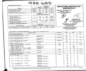
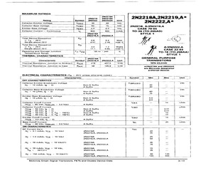
2N2218A anzzia | 2N2z19A 2N2218A,2N2219,A* Rating Symbol | 2N2222 | 2N2222A Unit * Collector-Emitter Voltage VcEO 30 40 Vde 2N2222,A Collector-Base Voltage VcBO 60 75 Vde 2N2218, A/2N221 9,A Emitter-Base Voltage VEBO 5.0 6.0 Vde CASE 79-04 Collector Current Continuous Ic 800 800 mAdc TO-39 (TO-205AD) 2N2218A STYLE 1 a Collector 2N2219,A | 2N2222,A Total Device Dissipation Pp 2 @ Tp = 28C 0.8 0.4 Watt Base Derate above 25C 4.57 2.28 mW/C 3 emit Total Device Dissipation Pp a @ Tr = 25C 3.0 1.2 Watts A/2N2222,A Derate above 25C 17.1 6.85 mWPC CASE 22-03 Operating and-Storage Junction Ty, Tstg -65 to +200 C TO-18 (TO-206AA) Temperature Range 3 STYLE 1 THERMAL CHARACTERISTICS an OND218A GENERAL PURPOSE Characteristic Symbol! | 2N2219,A | 2N2222,A | Unit TRANSISTORS Thermal Resistance, Junction to Ambient | Raja 219 437.5 C/W NPN SILICON Thermal Resistance, Junction to Case RaJc 58 145.8 CAW *2N2219A and 2N2222A are Motorola designated preferred devices. | Characteristic Symbo
 5 Pages, 384 KB, Scan
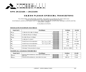
2N2218A - 2N2219A SILICON PLANAR EPITAXIAL TRANSISTORS The 2N2218A and 2N2219A are NPN transistors mounted in TO-39 metal case . They are designed for high-speed switching applications, And feature useful current gain over a wide range of collector current, low leakage currents and low saturation voltages. Compliance to RoHS ABSOLUTE MAXIMUM RATINGS Symbol Ratings VCEO Collector-Emitter Voltage VCBO Collector-Base Voltage VEBO Emitter-Base Voltage IC Collector Current PD Total Power Dissipation @ Tamb = 25 PD Total Power Dissipation @ Tcase= 25 TJ Junction Temperature TStg Storage Temperature range 2N2218A 2N2219A 2N2218A 2N2219A 2N2218A 2N2219A 2N2218A 2N2219A 2N2218A 2N2219A 2N2218A 2N2219A 2N2218A 2N2219A 2N2218A 2N2219A Value Unit 40 V 75 V 6 V 800 mA 0.8 Watts 3 Watts 175 C -65 to +200 C THERMAL CHARACTERISTICS Symbol Ratings RthJ-a Thermal Resistance, Junction to ambient in f
 3 Pages, 219 KB, Original
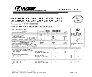
 JAN, JTX, JTXV, JANS QML DEVICES Processed per MIL-PRF-19500/251 NPN SWITCHING SILICON TRANSISTOR MAXIMUM RATINGS Ratings Symbol Collector-Emitter Voltage Collector-Base Voltage Emitter-Base Voltage Collector Current Total Power Dissipation 2N2218 2N2219 2N2218A; AL 2N2219A; AL 30 60 5.0 50 75 6.0 VCEO VCBO VEBO IC @ TA = +250C(1) @ TC = +250C(2) Operating & Storage Junction Temp. Range PT Top, Tstg 800 0.8 3.0 -55 to +200 Unit Vdc Vdc Vdc mAdc W W 0 C 2N2218, 2N2218A 2N2219, 2N2219A TO- 39 (TO-205AD) THERMAL CHARACTERISTICS Characteristics Thermal Resistance, Junction-to-Case 0 Symbol 0 RJC Max. 59 Unit C/mW 0 1) Derate linearly 4.6 mW/ C for TA > +25 C 2) Derate linearly 17.0 mW/0C for TC > +250C 2N2218AL, 2N2219AL TO-5 ELECTRICAL CHARACTERISTICS Characteristics Symbol Min. Max. Unit 2N2218, 2N2219 2N2218A, AL, 2N2219A, V(BR)CEO 30 50 2N2218, 2N2219 2N2218A, AL, 2N2219A, IEBO 10 10 10 Adc Adc ICES 10 10 Adc OFF CHARACTERISTICS Collector-Emitt
 2 Pages, 31 KB, Original
2N2218A anzzia | 222190 2N2218A,2N2219,A* Rating Symbol | 2N2222 | 2N2222A | Unit * Collector-Emitter Voltage VcEO 30 40 Vde 2N2222,A Collector-Base Voltage VcBo 60 75 Vde 2N2218, A/2N2219,A Emitter-Base Voltage VEBoO 5.0 6.0 Vdc CASE 79-04 Collector Current Continuous Ic 800 800 mAdc TO-39 (TO-205AD) 2N2218A STYLE 1 Coie 2N2219,A | 2N2222,A = Total Device Dissipation Pp ? a Ty = 25C 0.8 0.4 Watt fase Derate above 25C 4.57 2.28 mwrc 1 pent Total Device Dissipation Pp (a Te = 26C 3.0 1.2 Watts A/2N2222,A Derate above 25C 17.1 6.85 mwerc CASE 22-03 Operating and Storage Junction Ty. Tstg -65 to + 200 oF TO-18 (TO-206AA) Temperature Range 3 STYLE 1 THERMAL CHARACTERISTICS a OND2IBA GENERAL PURPOSE Characteristic Symbol | 2N2219,A | 2N2222,A | Unit TRANSISTORS Thermal Resistance, Junction to Ambient | Raya 219 437.5 C/W NPN SILICON Thermal Resistance, Junction to Case Rac 58 145.8 CW *&2N2219A and 2N2222A ELECTRICAL CHARACTERISTICS (Ta = 25C unless otherwise noted.) are Moto
 5 Pages, 187 KB, Scan
2N2218A JAN, JTX, JTXV 2N2218AL JAN, JTX, JTXV 2N2219, 2N2219A JAN, JTX, JTXV 2N2219AL JAN, JTX, JTXV MIL-PRF QPL DEVICES Processed per MIL-PRF-19500/251 NPN SWITCHING SILICON TRANSISTOR MAXIMUM RATINGS Ratings Collector-Emitter Voltage Collector-Base Voltage Emitter-Base Voltage Collector Current Total Power Dissipation @ TA = +250C(1) @ TC = +250C(2) Operating & Storage Junction Temperature Range Symbol 2N2218 2N2219 2N2218A; L 2N2219A; L Unit VCEO VCBO VEBO IC PT 30 60 5.0 50 75 6.0 800 Vdc Vdc Vdc mAdc 0.8 3.0 -65 to +200 W W 0 C TJ, Tstg 2N2218, 2N2218A 2N2219, 2N2219A TO- 39 (TO-205AD) THERMAL CHARACTERISTICS Characteristics Symbol Thermal Resistance, RJC Junction-to-Case 0 1) Derate linearly 4.6 mW/ C for TA > +250C 2) Derate linearly 17.0 mW/0C for TC > +250C Max. 0.059 Unit C/mW 0 2N2218AL, 2N2219AL TO-5 ELECTRICAL CHARACTERISTICS (TA = 250C unless otherwise noted) Characteristics Symbol Min. Max. Unit 2N2218, 2N2219 2N2218A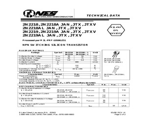 2 Pages, 25 KB, Original
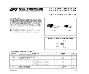
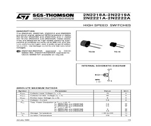
2 Pages, 25 KB, Original2N2218A-2N2219A 2N2221A-2N2222A HIGH SPEED SWITCHES DESCRIPTION The 2N2218A, 2N2219A, 2N2221A and 2N2222A are silicon planar epitaxial NPN transistors in Jedec TO-39 (for 2N2218A and 2N2219A) and in Jedec TO-18 (for 2N2221A and 2N2222A) metal cases. They are designed for high-speed switching applications at collector currents up to 500 mA, and feature useful current gain over a wide range of collector current, low leakage currents and low saturation voltages. 2N2218A/2N2219A approved to CECC 50002-100, 2N2221A/2N2222A approved to CECC 50002-101 available on request. TO-39 TO-18 INTERNAL SCHEMATIC DIAGRAM ABSOLUTE MAXIMUM RATINGS Symbol Parameter Value Unit V CBO Collector-base Voltage (I E = 0) 75 V V CEO Collector-emitter Voltage (I B = 0) 40 V V EBO Emitter-base Voltage (I C = 0) IC Pt o t 6 V 0.8 A 2N2219A 2N2222A 0.8 0.5 W W 2N2219A 2N2222A 3 1.8 W W Collector Current Total Power Dissipation at T amb 25 C for 2N2218A and for 2N2221A and at T
 8 Pages, 107 KB, Original
2N2218A-2N2219A 7 MicRoELECTROMIGS 2N2221A-2N2222A HIGH SPEED SWITCHES DESCRIPTION The 2N2?218A, 2N2219A, 2N2221A and 2N2222A are silicon planar epitaxial NPN transistors in Jedec TO-39 (for 2N2218A and 2N2219A) and in Jedec TO-18 (for 2N2221A and 2N2222A) metal cases. They are designed for high-speed switching appli cations at collector currents up to 500 mA, and tea- ture useful current gain over a wide range of collec- tor current, low leakage currents and low saturation voltages. & 2N2218A/2N2219A approved to CECC 50002-100, 2N2221AN2N2222A approved to CECC 50002101 available on request. TO-39 TO-18 INTERNAL SCHEMATIC DIAGRAM Cc B NPN S Gouy E ABSOLUTE MAXIMUM RATINGS Symbol Parameter Value Unit VcBo Gollecter-base Voltage (I_ = 0) 75 Vv VcEo Collector-emitter Voltage (Ip = 0) 40 V VeEBo Emitter-base Voltage (Ic = 0) 6 Vv le Collector Gurrent 0.8 A Prot Total Power Dissipation at Tamy < 25 C for 2N2218A and 2N2219A 0.8 WwW for 2N2221A and 2N2222A 0.5 Ww
 8 Pages, 154 KB, Scan
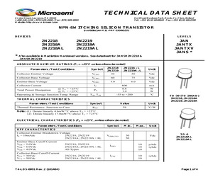
8) 620-2600 / Fax: (978) 689-0803 Website: http://www.microsemi.com Gort Road Business Park, Ennis, Co. Clare, Ireland Tel: +353 (0) 65 6840044 Fax: +353 (0) 65 6822298 NPN-SWITCHING SILICON TRANSISTOR Qualified per MIL-PRF-19500/251 DEVICES LEVELS 2N2218 2N2218A 2N2218AL 2N2219 2N2219A 2N2219AL * Also available in Radiation Hardened versions. JAN JANTX JANTXV JANS * See datasheet for JANSR2N2218 & JANSR2N2219 ABSOLUTE MAXIMUM RATINGS (TC = +25C unless otherwise noted) Collector-Emitter Voltage VCEO 2N2218 2N2219 30 Collector-Base Voltage VCBO 60 75 Vdc Emitter-Base Voltage VEBO 5.0 6.0 Vdc Parameters / Test Conditions Collector Current Symbol IC @ TA = +25C @ TC = +25C Operating & Storage Junction Temp. Range Total Power Dissipation 2N221A; L 2N2219A; L 50 Unit Vdc Top, Tstg 800 0.8 3.0 -55 to +200 mA W W C Symbol Value Unit RJC 59 C/W PT THERMAL CHARACTERISTICS Parameters / Test Conditions Thermal Resistance, Junction-to-Case TO-39 (TO-205AD) 2N2218, 2N2218A 2N2219, 2N
 5 Pages, 166 KB, Original
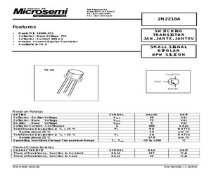
2N2218A Features * * * * * SWITCHING TRANSISTOR JAN, JANTX, JANTXV Meets MIL 19500 /251 Collector - Base Voltage 75V Collector - Current 800 mA Medium Current, Bipolar Transistor Available in TO-5 SMALL SIGNAL BIPOLAR NPN SILICON TO-39 Maximum Ratings RATING Collector - Emitter Voltage Collector - Base Voltage Emitter - Base Voltage Collector Current - Continuous Total Device Dissipation @ TA = 25 C Derate above 25 C Total Device Dissipation @ TC = 25 C Derate above 25 C Operating Junction&Storage Temperature Range SYMBOL VCEO VCBO VEBO IC PD T J, Tstg VALUE 50 75 6 800 0.8 4.6 3.0 17.0 - 55 to +200 UNIT Vdc Vdc Vdc mAdc WATTS mW/C WATTS mW/C C SYMBOL R JA R JC MAX 217 59 UNIT C/W C/W PD Thermal Characteristics CHARACTERISTIC Thermal Resistance, Junction to Ambient Thermal Resistance, Junction to Case MSCO933A 10-14-98 DSW2N2218A <-> (34724) 2N2218A Electrical Characteristics (TA = 25C unless otherwise noted) OFF CHARACTERISTIC Collector - Emitter Breakdown Voltage (1) (
 9 Pages, 167 KB, Original
2 1OM 200M {T 2N2216 S | P | 2N3498 8-232 | HSA 3.0W |C |200 4150 100 0 25 4120 50M 5.0 50M 50M |T 2N2217 S |N | 2N2218 8-108 | HSA O.8W JA [175 60 30 0 20 60 150M 0.4 150M 250M | T 2N2218 SN 8-108 | HSA 0.8W 7A 1175 60 30 oO 40 |120 150M 0.4 150M 250M |T 2N2218A |S |N 8-114 | HSS | 0.8W JA ]175 | 75 40 |O | 40 |120 70.154 0.3 {0.154 30 |E } 250M |T 2N2219 S|N 8-108 | HSA O.8W TA 1175 60 30 O 4100 | 300 150M 0.4 150M 250M |T 2N2219A |S [N 8-114 | HSS 0.8Ww }A [175 75 40 O j100 ;200 10.154 0.3 [O.15A 50 /E 300M |T 2N2220 S |N | 2N2222 8-108 | HSA O.5W |A [175 60 30 0 20 60 150M 9.4 150M 250M |T 2N2221 Ss |N 8-108 | HSA O.5wWw |A [175 60 30 oO 40 $120 150M 0.4 150M 250M |T 2N2221A [S| N 8-114 } HSS O.5W JA 7175 75 40 oO 40 }120 |0.15A 0.3 [0.154 30 JE 250M |T 2N2222 S|N 8-108 | HSA 0.5W YA 1175 60 30 oO |100 | 300 150M 0.4 150M 250M {T 2N2222A |S {N 8-114 | HSS | O.5W {A J175 | 75 40 {O |100 |300 |0.15A 0.3 [0.154 50 |E | 300M }T 2N2223 SIN 11-6 DFA 500M }A |200 | 100 80 R 50 | 200 10M 1.2 50M 40 /
 6 Pages, 276 KB, Scan