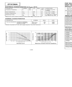
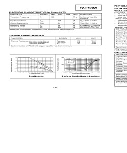
ZTX790A ELECTRICAL CHARACTERISTICS (at Tamb = 25C) PARAMETER SYMBOL MIN. Transition Frequency fT 100 Input Capacitance Cibo Output Capacitance Switching Times TYP. MAX. UNIT CONDITIONS. MHz IC=-50mA, VCE=-5V f=50MHz 225 pF VEB=-0.5V, f=1MHz Cobo 24 pF VCB=-10V, f=1MHz ton toff 35 600 ns ns IC=-500mA, IB1=-50mA IB2=-50mA, VCC=-10V *Measured under pulsed conditions. Pulse width=300s. Duty cycle 2% THERMAL CHARACTERISTICS PARAMETER SYMBOL Rth(j-amb)1 Rth(j-amb)2 Rth(j-case) Thermal Resistance: Junction to Ambient1 Junction to Ambient2 Junction to Case MAX. UNIT 175 116 70 C/W C/W C/W Device mounted on P.C.B. with copper equal to 1 sq. Inch minimum. ZTX790A ISSUE 2 APRIL 94 FEATURES * 40 Volt VCEO * Gain of 200 at IC=1 Amps * Very low saturation voltage APPLICATIONS * Darlington replacement * Siren driver * Battery powered circuits * Motor drivers C B E E-Line TO92 Compatible ABSOLUTE MAXIMUM RATINGS. PARAMETER SYMBOL VALUE UNIT V Collector-Base Voltage VCBO -50 Collector-Emitter Voltage
 4 Pages, 85 KB, Original
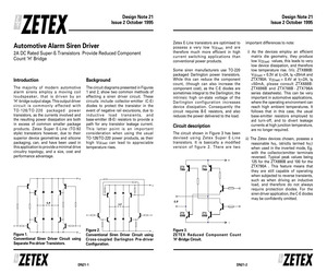
mportant differences to note: i) As the devices employ an efficient matrix die geometry, they produce low VCE(sat) values, this leads to very low device dissipation, and therefore low temperature rise. (Viz. ZTX690B: VCE(sat) = 0.3V at IC=2A, IB =20mA and ZTX790A: VCE(sat) = 0.4V at IC=2A, IB =50mA, please consult ZTX688BZTX696B and ZTX788B - ZTX796A series datasheets). This can be very important in automotive applications, where the operating environment can reach high ambient temperatures. It follows that in this case, the usual base-emitter resistors employed to aid turn-off, and to divert leakage currents at high junction temperature, are no longer required. Some siren manufacturers use TO-220 packaged Darlington power transistors. While this can reduce the component count, (though can also increase the component cost), as the C-E diodes are sometimes integral to the Darlington, the intrinsic high on-state voltage of the Darlington configuration increases device dissipation. Consequently the
 4 Pages, 113 KB, Original
ZTX790A ELECTRICAL CHARACTERISTICS (at Tamb = 25C) PARAMETER SYMBOL MIN. Transition Frequency fT 100 Input Capacitance Cibo Output Capacitance Switching Times TYP. MAX. UNIT CONDITIONS. MHz IC=-50mA, VCE=-5V f=50MHz 225 pF VEB=-0.5V, f=1MHz Cobo 24 pF VCB=-10V, f=1MHz ton toff 35 600 ns ns IC=-500mA, IB1=-50mA IB2=-50mA, VCC=-10V *Measured under pulsed conditions. Pulse width=300s. Duty cycle 2% THERMAL CHARACTERISTICS PARAMETER SYMBOL Rth(j-amb)1 Rth(j-amb)2 Rth(j-case) Thermal Resistance: Junction to Ambient1 Junction to Ambient2 Junction to Case MAX. UNIT 175 116 70 C/W C/W C/W Device mounted on P.C.B. with copper equal to 1 sq. Inch minimum. ZTX790A ISSUE 2 APRIL 94 FEATURES * 40 Volt VCEO * Gain of 200 at IC=1 Amps * Very low saturation voltage APPLICATIONS * Darlington replacement * Siren driver * Battery powered circuits * Motor drivers C B E E-Line TO92 Compatible ABSOLUTE MAXIMUM RATINGS. PARAMETER SYMBOL VALUE UNIT V Collector-Base Voltage VCBO -50 Collector-Emitter Voltage
 3 Pages, 65 KB, Original
 6 6 6 6 6 CRD-E5.6mA CRD-F5.6mA VNP5N07 GBU6D GBU6J W06 BZYC6V2 BZX6V2 BZX6V8 BZYC6V8 47-2610 47-2640 47-0402 47-2800 47-2802 47-3196 47-3018 47-3060 47-3062 47-3020 427 427 437 429 429 428 426 426 426 426 85 85 88 90 92 93 94 97 98 100 BAT85 BFX85 BFX88 ZTX790A MPSA92 BDW93C BDW94C TIS97 BYW98-200 BR100 47-3108 81-0116 81-0118 81-0242 81-0146 81-0110 81-0112 81-0008 47-3834 47-3264 427 432 432 433 432 433 434 431 427 430 1 1 2 2 2 2 2 2 2 2 1N5408 1N5820 CRD-E2.0mA W02 2KBP02 BZYC2V7 2KBP04 2SK1119 2SB817 2SB1037 47-3152 47-2546 47-2602 47-3192 47-3200 47-3000 47-3202 47-0304 81-0342 81-0298 427 428 427 428 428 426 428 437 435 435 6 6 7 7 7 7 8 8 8 8 BTA06-600BW BTA06-600T VNP7N04 BZX7V5 BZYC7V5 STGP7NB60HD KBU8D KBU8K W08 BZX8V2 47-3396 47-3390 47-0404 47-3064 47-3022 47-0456 47-3214 47-3216 47-3198 47-3066 430 430 437 426 426 437 429 429 428 426 100 102 103 104 106 107 107 107 107 108 BYW100-200 KBPC102 Z0103MA KBPC104 TIC106D BC107 BC107B BS107 Z0107MA BC108 47-3836 47-3206 47-3406 47-3208 4
 16 Pages, 404 KB, Original
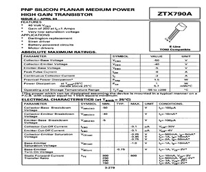
ZTX790A ISSUE 2 - APRIL 94 FEATURES * 40 Volt Vogg * Gain of 200 at |.=1 Amps * Very low saturation voltage APPLICATIONS * Darlington replacement Cc * Siren driver BE * Battery powered circuits . * Motor drivers E-Line TOS2 Compatible ABSOLUTE MAXIMUM RATINGS. PARAMETER SYMBOL VALUE UNIT Collector-Base Voltage Vepo -50 Vv Collector-Emitter Voltage Vceo -40 Emitter-Base Voltage Veso a) Vv Peak Pulse Current lem 6 A Continuous Collector Current le -2 A Practical Power Dissipation* totp 1.5 Ww Power Dissipation at T,,,,4=25C rot 1 Ww derate above 25C 5.7 mWwPc Operating and Storage Temperature Range TT stg -55 to +200 c *The power which can be dissipated assuming the device is mounted in a typical manner on a P.C.B. with copper equal to 1 inch square minimum ELECTRICAL CHARACTERISTICS (at Tamb = 25C) PARAMETER SYMBOL | MIN. | TYP. | MAX. | UNIT | CONDITIONS. Collector-Base Breakdown Vieryczo (| -90 Vv I-=-100pA Voltage Collector-Emitter Breakdown | Vigayceg | -40 Vv i=-10mA* Voltage Emitter-Base Bre
 3 Pages, 96 KB, Scan
ch the battery pack to BAT+ and BAT-. 4. Connect the charging supply to TB1 (DC+, DC-). The combined charging and system load should not exceed the IMAX limit of 2.5A. Rev. B Board 4 DV2031S2 DV2031S2 Board Schematic D6A VDC 1 2 VDC+ 1N5821 TB1 R21 D6B Q3 ZTX790A SBL845DI 20K Q1 MTP23P06V R6 L1 10K 200H 1 D1 1N4148 C6 R4 1000F 35V 10K D2 1N4744 U2 102K 1% 2 Cell 3 Cell 261K 1% C14 470F 35v TB2 BAT BAT+ BAT- 6 Cell 1 2 3 4 TEM 0.1F R20 2 4 6 8 0.10 2W JP5 Q4 ZTX790A C9 10F 4 Cell R14 C15 100K 1000pF C3 154K 1% TEMTEM+ R7 +5V 78L05 52.3K 1% 1 C4 IN OUT GND D7A SBL845DI R17 R15 R16 D7B 1N5821 Q2 2N3904 10F 1 3 5 7 1 C7 10F 35V R22 43_OHMS JP3 JP2 JP1 TSEL DSEL QSEL Q5 3 2 1 3 2 1 R12 R8 2N3904 3 2 1 220 49.9K 1% +5V +5V JP4 IGSEL R10 10K R11 R9 10K 10K C2 R5 C5 0.1F 62K 0.1F R19 464K 1% 0.01F 3 2 1 R18 1K C13 U1 LED3 C11 2 2 LED2 LED1 C8 16 15 14 13 12 11 10 9 LED2/DSEL LED1/TSEL MOD VCC VSS COM LED3/QSEL TPWM TMTO FLOAT BAT VCOMP ICOMP IGSEL SNS TS +5V R2 6.81K 1% R3 3.74K 1% 1 2 3 4 5
 9 Pages, 91 KB, Original
erSOT series. The FMMT718 chip is also available in the E-Line (enhanced TO92) package). Device BVCEO IC(DC) ICM hFE @IC/VCE VCE(sat) (max.) @IC/IB Package ZTX788B 15 3 8 300 min 2A/2V 450mV 2A/10mA E-Line ZTX789A 25 3 8 200 min 2A/2V 450mV 2A/20mA E-Line ZTX790A 40 2 6 200 min 1A/2V 450mV 1A/10mA E-Line ZTX949 30 4.5 20 140(typ) 5A/1V 320mV 5A/300mA E-Line ZTX951 60 4 15 120(typ) 4A/1V 300mV 4A/400mA E-Line Table 2. PNP Transistors for Fast Chargers 1 to 4A. (Selected from the ZTX788B - ZTX976A, and ZTX950 series. These devices are available in the SOT223 surface mount package - prefixed FZT eg FZT788B). Device BVCEO IC(DC ) ICM hFE @IC/VCE VCE(sat) (max.) @IC/IB Package ZBD949 30 5 20 140(typ) 5A/1V 450mV 5A/300mA TO126 ZBD953 100 4 10 90(typ) 3A/1V 470mV 4A/400mA TO126 Table 3. PNP Transistors for Linear and Switched Mode High Current (5A) Fast Chargers. AN26 - 6 AN26 - 7 Application Note 26 Issue 1 April 1996 Figure 4 shows the turn-off produced with a passive turn-off circuit - a resistor. T
 7 Pages, 232 KB, Original
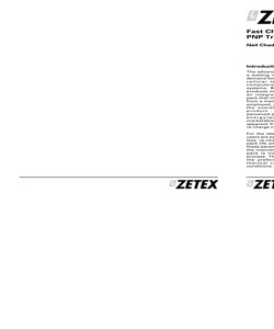
or an Automotive application, but similar circuits should also find use in industrial control systems. Similar circuits for higher current applications are possible with a change to the output device. For example, the ZTX751 2A rated PNP, or the high gain ZTX790A could be used for load currents of up to 2A, while the ZTX951 allows operation to over 3A. 560 560 27K ZTX300 1F 0.1 470 Figure 1 12V Latch Circuit. Since the ZTX300 is now on, when the p u s h - b u t t o n i s r e l e a s e d t h e 1F capacitor will be discharged through the transistor via the bleed resistor. If the push-button is operated again it will connect this discharged capacitor to the bias network of the ZTX300 turning it and thus the output off. Any excess energy stored in the solenoid will be DN27 - 1 DN 27 - 2 1N4000 1A SOLENOID Design Note 27 Issue 1 February 1996 Design Note 27 Issue1 February 1996 +12V 12V Solenoid Driver/Latch Single Switch Operated, High Current High Side Switch 270 ZTX550 ZTX550 This circuit has been
 2 Pages, 74 KB, Original
ZTX790A PNP SILICON PLANAR MEDIUM POWER HIGH GAIN TRANSISTOR FXT790A ELECTRICAL CHARACTERISTICS (at Tamb = 25C) PARAMETER SYMBOL MIN. Transition Frequency fT 100 Input Capacitance Cibo Output Capacitance Switching Times TYP. MAX. UNIT CONDITIONS. MHz IC=-50mA, VCE=-5V f=50MHz 225 pF VEB=-0.5V, f=1MHz Cobo 24 pF VCB=-10V, f=1MHz ton toff 35 600 ns ns IC=-500mA, IB1=-50mA IB2=-50mA, VCC=-10V *Measured under pulsed conditions. Pulse width=300s. Duty cycle 2% THERMAL CHARACTERISTICS PARAMETER SYMBOL Thermal Resistance: Junction to Ambient1 Junction to Ambient2 Junction to Case Rth(j-amb)1 Rth(j-amb)2 Rth(j-case) MAX. UNIT 175 116 70 C/W C/W C/W ISSUE 2 APRIL 94 FEATURES * 40 Volt VCEO * Gain of 200 at IC=1 Amps * Very low saturation voltage APPLICATIONS * Darlington replacement * Siren driver * Battery powered circuits * Motor drivers B C E E-Line TO92 Compatible ABSOLUTE MAXIMUM RATINGS. PARAMETER SYMBOL VALUE UNIT Collector-Base Voltage VCBO -50 V Collector-Emitter Voltage VCEO -40 V Emitter-Base V
 2 Pages, 68 KB, Original
C A IC A fT min. (*typ) MHz Ptot @ 25C W 300 400 300 300 400 300 400 1 2 0.2 1 1 1 0.2 150 150 100 155 150 140 130 1 1 1 1 1 1 1 ZTX1048A ZTX689B ZTX618 ZTX1051A ZTX690B ZTX1053A ZTX694B 200 250 200 250 2 0.5 1 0.5 100 135 100 100 1 1 1 1 ZTX789A ZTX1149A ZTX790A ZTX792A hFE @ min. Mftrs. List No. 211060 Order Multiple=5 Price Each Mftrs. List No. Order Code 5+ 25+ 100+ 1K+ 5K+ ZTX618 ZTX689B 952-6528 952-5602 ZTX690B ZTX694B 952-5947 952-5610 ZTX789A ZTX790A 952-6170 952-6188 ZTX792A ZTX1048A 952-6137 952-6544 ZTX1051A ZTX1053A ZTX1149A 952-6552 952-6390 952-6781 0.93 2.03 0.76 1.69 1.22 2.01 2.01 1.71 2.01 1.86 2.01 0.57 1.31 0.51 1.09 0.92 1.29 1.29 1.30 1.29 1.18 1.29 0.41 0.83 0.41 0.69 0.66 0.82 0.82 0.77 0.74 0.68 0.74 0.32 0.72 0.40 0.60 0.60 0.72 0.72 0.60 0.58 0.52 0.58 0.25 0.54 0.38 0.44 0.46 0.52 0.52 0.47 0.45 0.40 0.45 E-Line, TO-92 High Voltage, VCEO 300V VCEO max. V 300 300 400 400 400 400 400 IC max. A 0.5 3 0.2 0.3 0.5 1 1 hFE @ min. 50 100 100 100 40 5 4 Ptot IC V
 144 Pages, 26045 KB, Original
currents of 9.4mA, 43mA and 170mA respectively. Figure 11 shows how the efficiency varies with input voltage for the IB=43mA option. Higher output current designs are possible with larger die transistors from the Zetex range, such as the ZTX788B, ZTX789A, ZTX790A, ZTX948 and ZTX949. For a comprehensive listing please refer to Semiconductor Data Books one and two. AN22 - 5 Application Note 22 Issue 1 May 1996 Application Note 22 Issue 1 May 1996 +5V measurements for the ZTX1048A - for example, at a collector current of 1A and a forced gain of 200, a turn-off charge of 900pC is required to neutralise stored charge and eliminate storage time effects. 100n ZTX1048A C To Oscilloscope Q1 +5V Input RB 0V 0V Figure 5. Capacitive Speed-up method/Circuit to Determine Minimum Value of Turn-Off Charge of a Bipolar Transistor. Stored Charge (C) IC/IB=50 RC IC/IB=100 IC/IB=150 IC/IB=200 10n [Note 1: Appendix A also includes some ancillary material on the minimum amount of trigger charge necessary for pulse cir
 16 Pages, 308 KB, Original
ch the battery pack to BAT+ and BAT-. 4. Connect the charging supply to TB1 (DC+, DC-). The combined charging and system load should not exceed the IMAX limit of 2.2A. Rev. B Board 4 DV2031S2 DV2031S2 Board Schematic D6A VDC 1 2 VDC+ 1N5821 TB1 R21 D6B Q3 ZTX790A SBL845DI 20K Q1 MTP23P06V R6 L1 10K 200H 1 D1 1N4148 C6 R4 1000F 35V 10K D2 1N4744 U2 102K 1% 2 Cell 3 Cell 261K 1% C14 470F 35v TB2 BAT BAT+ BAT- 6 Cell 1 2 3 4 TEM 0.1F R20 2 4 6 8 0.12 2W JP5 Q4 ZTX790A C9 10F 4 Cell R14 C15 100K 1000pF C3 154K 1% TEMTEM+ R7 +5V 78L05 52.3K 1% 1 C4 IN OUT GND D7A SBL845DI R17 R15 R16 D7B 1N5821 Q2 2N3904 10F 1 3 5 7 1 C7 10F 35V R22 43_OHMS JP3 JP2 JP1 TSEL DSEL QSEL Q5 3 2 1 3 2 1 R12 R8 2N3904 3 2 1 220 49.9K 1% +5V +5V JP4 IGSEL R10 10K R11 R9 10K 10K C2 R5 C5 0.1F 62K 0.1F R19 464K 1% 0.01F 3 2 1 R18 1K C13 U1 LED3 C11 2 2 LED2 LED1 C8 16 15 14 13 12 11 10 9 LED2/DSEL LED1/TSEL MOD VCC VSS COM LED3/QSEL TPWM TMTO FLOAT BAT VCOMP ICOMP IGSEL SNS TS +5V R2 6.81K 1% R3 3.74K 1% 1 2 3 4 5
 8 Pages, 87 KB, Original
2-ZTX788B 522-ZTX788A 522-FZT788BTA 522-FMMT718TA 522-FZT948TA 522-ZTX749 522-ZTX1149A 522-FZT749TA 522-FZT1149ATA 522-FMMT549TA 522-FMMT589TA 522-ZTX549 522-FZT549TA 522-ZXTP2008ZTA 522-ZTX949 522-ZXT790AKTC 522-FMMT591ATA 522-FCX591ATA 522-FMMT720TA 522-ZTX790A 522-FCX790ATA 522-ZXT13P40DE6TA 522-FCX1151ATA 522-FZT1151ATA 522-BCW68HTA 522-ZTX550 522-FZT951TA 522-ZX5T955GTA 17.5 75 5 5 2.75 2.75 250 300 - 5 1 0.24 0.44 5 5 100 250 522-ZXTD4591E6TA Package VCEO (V) IC (A) PD (W) FMMT717TA ZXT13P12DE6TA FZT968TA ZTX788B ZTX788A FZT788BTA FMMT718TA FZT948TATA ZTX749 ZTX1149A FZT749TA FZT1149ATA FMMT549TA FMMT589TA ZTX549 FZT549TA ZXTP2008ZTA ZTX949 ZXT790AKTC FMMT591ATA FCX591ATA FMMT720TA ZTX790A FCX790ATA ZXT13P40DE6TA FCX1151ATA FZT1151ATA BCW68HTA ZTX550 FZT9511TA ZX5T955GTA SOT-23 SOT-23-6 SOT-223 E-Line E-Line SOT-223 SOT-23 SOT-223 E-Line E-Line SOT-223 SOT-223 SOT-23 SOT-23 E-Line SOT-223 SOT-89 E-Line DPAK SOT-23 SOT-89 SOT-23 E-Line SOT-89 SOT-23-6 SOT-89 SOT-223 SOT-23 E-Lin
 1 Pages, 222 KB, Original
* * * Bipolar Transistor ZTX788B/ZTX Zetex Inc. ZTX788B/ZTX ZETEX.SLB * * * Tech Type Device Type Generic Name Mfg. Name Symbol Name Library Model Package New for 8.0 Bipolar Transistor ZTX789A/ZTX Zetex Inc. ZTX789A/ZTX ZETEX.SLB * * * Bipolar Transistor ZTX790A/ZTX Zetex Inc. ZTX790A/ZTX ZETEX.SLB * * * Bipolar Transistor ZTX792A/ZTX Zetex Inc. ZTX792A/ZTX ZETEX.SLB * * * Bipolar Transistor ZTX795A/ZTX Zetex Inc. ZTX795A/ZTX ZETEX.SLB * * * Bipolar Transistor ZTX796A/ZTX Zetex Inc. ZTX796A/ZTX ZETEX.SLB * * * Bipolar Transistor ZTX849/ZTX Zetex Inc. ZTX849/ZTX ZETEX.SLB * * * Bipolar Transistor ZTX851/ZTX Zetex Inc. ZTX851/ZTX ZETEX.SLB * * * Bipolar Transistor ZTX869/ZTX Zetex Inc. ZTX869/ZTX ZETEX.SLB * * * Bipolar Transistor ZTX869/ZTX Zetex Inc. ZTX869/ZTX ZETEX.SLB * * * Bipolar Transistor ZTX948/ZTX Zetex Inc. ZTX948/ZTX ZETEX.SLB * * * Bipolar Transistor ZTX949/ZTX Zetex Inc. ZTX949/ZTX ZETEX.SLB * * * Bipolar Transistor ZTX951/ZTX Zetex Inc. ZTX951/ZTX ZETEX.SLB * * * Bipol
 573 Pages, 724 KB, Original
td) X (e) China Green Sn N/A 260 ZTX788B EP3 X X (DC Ltd) X (e) China Green Sn N/A 260 ZTX788BSTZ EP3 X X (DC Ltd) X (e) China Green Sn N/A 260 ZTX789A EP3 X X (DC Ltd) X (e) China Green Sn N/A 260 ZTX789ASTOA EP3 X X (DC Ltd) X (e) China Green Sn N/A 260 ZTX790A EP3 X X (DC Ltd) X (e) China Green Sn N/A 260 ZTX790ASTZ EP3 X X (DC Ltd) X (e) China Green Sn N/A 260 ZTX792A EP3 X X (DC Ltd) X (e) China Green Sn N/A 260 ZTX792ASTZ EP3 X X (DC Ltd) X (e) China Green Sn N/A 260 ZTX795A EP3 X X (DC Ltd) X (e) China Green Sn N/A 260 ZTX795ASTZ EP3 X X (DC Ltd) X (e) China Green Sn N/A 260 ZTX796A EP3 X X (DC Ltd) X (e) China Green Sn N/A 260 ZTX796ASTOB EP3 X X (DC Ltd) X (e) China Green Sn N/A 260 ZTX849 EP3 X (DC Ltd) X Lead in High Temp Solder (50) China RoHS High Temp Solder Sn N/A 260 ZTX849STZ EP3 X (DC Ltd) X Lead in High Temp Solder (50) China RoHS High Temp Solder Sn N/A 260 ZTX851 EP3 X (DC Ltd) X Lead in High Temp Solder (50) China RoHS High Temp Solder Sn N/A 260 ZTX851STZ EP3 X
 98 Pages, 475 KB, Original