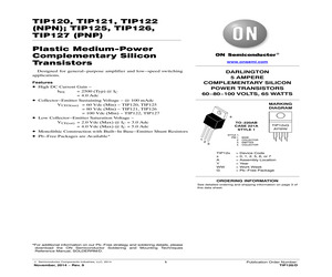
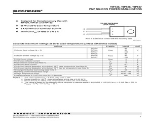
TIP125, TIP126, TIP127 (PNP) Plastic Medium-Power Complementary Silicon Transistors www.onsemi.com Designed for general-purpose amplifier and low-speed switching applications. Features * High DC Current Gain - = 2500 (Typ) @ IC = 4.0 Adc Collector-Emitter Sustaining Voltage - @ 100 mAdc VCEO(sus) = 60 Vdc (Min) - TIP120, TIP125 = 80 Vdc (Min) - TIP121, TIP126 = 100 Vdc (Min) - TIP122, TIP127 Low Collector-Emitter Saturation Voltage - VCE(sat) = 2.0 Vdc (Max) @ IC = 3.0 Adc = 4.0 Vdc (Max) @ IC = 5.0 Adc Monolithic Construction with Built-In Base-Emitter Shunt Resistors Pb-Free Packages are Available* hFE * * * * DARLINGTON 5 AMPERE COMPLEMENTARY SILICON POWER TRANSISTORS 60-80-100 VOLTS, 65 WATTS MARKING DIAGRAM 4 TO-220AB CASE 221A STYLE 1 1 2 3 STYLE 1: PIN 1. 2. 3. 4. TIP12x x A Y WW G TIP12xG AYWW BASE COLLECTOR EMITTER COLLECTOR = Device Code = 0, 1, 2, 5, 6, or 7 = Assembly Location = Year = Work Week = Pb-Free Package ORDERING INFORMATION See detailed ordering and shipping inf
 7 Pages, 135 KB, Original
TIP125, TIP126, TIP127 (PNP) Plastic Medium-Power Complementary Silicon Transistors www.onsemi.com Designed for general-purpose amplifier and low-speed switching applications. Features * High DC Current Gain - = 2500 (Typ) @ IC = 4.0 Adc Collector-Emitter Sustaining Voltage - @ 100 mAdc VCEO(sus) = 60 Vdc (Min) - TIP120, TIP125 = 80 Vdc (Min) - TIP121, TIP126 = 100 Vdc (Min) - TIP122, TIP127 Low Collector-Emitter Saturation Voltage - VCE(sat) = 2.0 Vdc (Max) @ IC = 3.0 Adc = 4.0 Vdc (Max) @ IC = 5.0 Adc Monolithic Construction with Built-In Base-Emitter Shunt Resistors Pb-Free Packages are Available* hFE * * * * DARLINGTON 5 AMPERE COMPLEMENTARY SILICON POWER TRANSISTORS 60-80-100 VOLTS, 65 WATTS MARKING DIAGRAM 4 TO-220AB CASE 221A STYLE 1 1 2 3 STYLE 1: PIN 1. 2. 3. 4. TIP12x x A Y WW G TIP12xG AYWW BASE COLLECTOR EMITTER COLLECTOR = Device Code = 0, 1, 2, 5, 6, or 7 = Assembly Location = Year = Work Week = Pb-Free Package ORDERING INFORMATION See detailed ordering and shipping inf
 8 Pages, 289 KB, Original
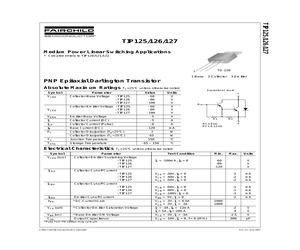
TIP125/TIP126/TIP127 PNP Epitaxial Darlington Transistor * Medium Power Linear Switching Applications * Complementary to TIP120/121/122 Equivalent Circuit C B TO-220 1 R1 1.Base 2.Collector Absolute Maximum Ratings* Symbol VCBO VCEO 3.Emitter R1 @ 8kW R2 @ 0.12k W R2 E T a = 25C unless otherwise noted Collector-Base Voltage Parameter : TIP125 : TIP126 : TIP127 Collector-Emitter Voltage : TIP125 : TIP126 : TIP127 Ratings - 60 - 80 - 100 Units V V V - 60 - 80 - 100 V V V VEBO Emitter-Base Voltage -5 V IC Collector Current (DC) -5 A ICP Collector Current (Pulse) -8 A IB Base Current (DC) - 120 mA PC Collector Dissipation (Ta=25C) 2 Collector Dissipation (TC=25C) 65 W W TJ Junction Temperature 150 C TSTG Storage Temperature - 65 ~ 150 C * These ratings are limiting values above which the serviceability of any semiconductor device may be impaired. (c) 2007 Fairchild Semiconductor Corporation TIP125/TIP126/TIP127 Rev. 1.0.0 www.fairchildsemi.com 1 TIP125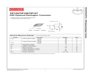 5 Pages, 536 KB, Original
5 Pages, 536 KB, OriginalTIP125, TIP126, TIP127 (PNP) Plastic Medium-Power Complementary Silicon Transistors www.onsemi.com Designed for general-purpose amplifier and low-speed switching applications. Features * High DC Current Gain - = 2500 (Typ) @ IC = 4.0 Adc Collector-Emitter Sustaining Voltage - @ 100 mAdc VCEO(sus) = 60 Vdc (Min) - TIP120, TIP125 = 80 Vdc (Min) - TIP121, TIP126 = 100 Vdc (Min) - TIP122, TIP127 Low Collector-Emitter Saturation Voltage - VCE(sat) = 2.0 Vdc (Max) @ IC = 3.0 Adc = 4.0 Vdc (Max) @ IC = 5.0 Adc Monolithic Construction with Built-In Base-Emitter Shunt Resistors Pb-Free Packages are Available* hFE * * * * DARLINGTON 5 AMPERE COMPLEMENTARY SILICON POWER TRANSISTORS 60-80-100 VOLTS, 65 WATTS MARKING DIAGRAM 4 TO-220AB CASE 221A STYLE 1 1 2 3 STYLE 1: PIN 1. 2. 3. 4. TIP12x x A Y WW G TIP12xG AYWW BASE COLLECTOR EMITTER COLLECTOR = Device Code = 0, 1, 2, 5, 6, or 7 = Assembly Location = Year = Work Week = Pb-Free Package ORDERING INFORMATION See detailed ordering and shipping inf
 8 Pages, 145 KB, Original
TIP125, TIP126, TIP127 (PNP) Preferred Devices Plastic Medium-Power Complementary Silicon Transistors http://onsemi.com Designed for general-purpose amplifier and low-speed switching applications. Features *High DC Current Gain hFE = 2500 (Typ) @ IC = 4.0 Adc *Collector-Emitter Sustaining Voltage - @ 100 mAdc VCEO(sus) = 60 Vdc (Min) - TIP120, TIP125 = 80 Vdc (Min) - TIP121, TIP126 = 100 Vdc (Min) - TIP122, TIP127 *Low Collector-Emitter Saturation Voltage VCE(sat) = 2.0 Vdc (Max) @ IC = 3.0 Adc = 4.0 Vdc (Max) @ IC = 5.0 Adc *Monolithic Construction with Built-In Base-Emitter Shunt Resistors *Pb-Free Packages are Available* DARLINGTON 5 AMPERE COMPLEMENTARY SILICON POWER TRANSISTORS 60-80-100 VOLTS, 65 WATTS MARKING DIAGRAM 4 1 TO-220AB CASE 221A STYLE 1 2 TIP12xG AYWW 3 TIP12x x A Y WW G = Device Code = 0, 1, 2, 5, 6, or 7 = Assembly Location = Year = Work Week = Pb-Free Package ORDERING INFORMATION See detailed ordering and shipping information in the package dimensions section on
 7 Pages, 107 KB, Original
TIP125/126/127 TIP125/126/127 SEMIHOW REV.A0,Oct 2007 TIP125/126/127 TIP125/126/127 Monolithic Construction With Built In Base-Emitter Shunt Resistors PNP Epitaxial Silicon Darlington Transistor - High DC Current Gain : hFE=1000 @ VCE= -4V, IC= -3A (Min.) - Collector-Emitter Sustaining Voltage - Low Collector-Emitter Saturation Voltage - Industrial Use - Complementary to TIP120/121/122 Equivalent Circuit Absolute Maximum Ratings CHARACTERISTICS Ta=25 unless otherwise noted SYMBOL RATING UNIT : TIP125 : TIP126 : TIP127 VCBO -60 -80 -100 V V V Collector-Emitter Voltage : TIP125 : TIP126 : TIP127 VCEO -60 -80 -100 V V V Emitter-Base Voltage Collector Current(DC) Collector Current(Pulse) Base Current Collector Dissipation(Ta=25) Collector Dissipation(Tc=25) Junction Temperature Storage Temperature VEBO IC ICP IB PC PC TJ TSTG Collector-Base Voltage Electrical Characteristics -5 -5 -8 -120 2 65 150 -65~150 V A A W W TO-220 1. Base 2. Col
 5 Pages, 501 KB, Original
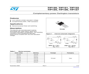
TIP125, TIP126, TIP127 Complementary power Darlington transistors Features Low collector-emitter saturation voltage Complementary NPN - PNP transistors Applications General purpose linear and switching 3 1 Description TO-220 The devices are manufactured in planar technology with "base island" layout and monolithic Darlington configuration. The resulting transistors show exceptional high gain performance coupled with very low saturation voltage. Figure 1. Internal schematic diagrams NPN: R1= 7 K R2= 70 Table 1. 2 PNP: R1= 16 K R2= 60 Device summary Order codes Marking TIP120 TIP120 TIP121 TIP121 TIP122 TIP122 TIP125 TIP125 TIP126 TIP126 TIP127 TIP127 November 2008 Rev 4 Package Packaging TO-220 Tube 1/13 www.st.com 13 Content TIP120, TIP121, TIP122, TIP125, TIP126, TIP127 Content 1 Electrical ratings . . . . . . . . . . . . . . . . . . . . . . . . . . . . . . . . . . . . . . . . . . . . 3 2 Electrical characteristics . . . . . . . . . . . . . . . . . . . . .
 14 Pages, 602 KB, Original
TIP125, TIP126, TIP127 (PNP) Preferred Devices Plastic Medium-Power Complementary Silicon Transistors Designed for general-purpose amplifier and low-speed switching applications. Features *High DC Current Gain hFE = 2500 (Typ) @ IC = 4.0 Adc *Collector-Emitter Sustaining Voltage - @ 100 mAdc VCEO(sus) = 60 Vdc (Min) - TIP120, TIP125 = 80 Vdc (Min) - TIP121, TIP126 = 100 Vdc (Min) - TIP122, TIP127 *Low Collector-Emitter Saturation Voltage VCE(sat) = 2.0 Vdc (Max) @ IC = 3.0 Adc = 4.0 Vdc (Max) @ IC = 5.0 Adc *Monolithic Construction with Built-In Base-Emitter Shunt Resistors *Pb-Free Packages are Available* DARLINGTON 5 AMPERE COMPLEMENTARY SILICON POWER TRANSISTORS 60-80-100 VOLTS, 65 WATTS MARKING DIAGRAM 4 1 TO-220AB CASE 221A STYLE 1 2 TIP12xG AYWW 3 TIP12x x A Y WW G = Device Code = 0, 1, 2, 5, 6, or 7 = Assembly Location = Year = Work Week = Pb-Free Package ORDERING INFORMATION See detailed ordering and shipping information in the package dimensions section on page 2 of this dat
 4 Pages, 76 KB, Original
6042 2N6041 2N6041 TIP127 3-497 3-873 3-873 3-89 3-89 3-89 3-900 2SB531 2SB532 2SB536 2SB537 2SB539 2SB541 2SB546 MJ15016 MJ15016 TIP32C TIP32C MJ15002 MJ15002 MJE15031 3-5 3-5 3-873 3-873 3-497 3-497 3-684 2SB677 2SB679 2SB681 2SB686 2SB688 2SB689 2SB690 TIP125 TIP117 MJ15002 TIP42C MJE15029 TIP42C TIP42C 3-900 3-895 3-497 3-883 3-684 3-883 3-883 2SB546 2SB547 2SB548 2SB549 2SB552 2SB553 2SB554 MJE15031 MJE15031 2N4920 2N4920 MJ15025 2N6107 MJ15025 3-684 3-684 3-34 3-34 3-509 3-101 3-509 2SB691 2SB692 2SB693 2SB694 2SB695 2SB696 2SB697 MJE4352 MJE4352 2N6287 MJ11015 MJE4352 MJ15002 MJ15002 3-632 3-632 3-112 3-478 3-632 3-497 3-497 2SB555 2SB556 2SB557 2SB558 2SB559 2SB565 2SB566 MJ15012 MJ15012 MJ15002 2N5880 2N4918 TIP32B TIP32C 3-502 3-502 3-497 3-77 3-34 3-873 3-873 2SB707 2SB708 2SB711 2SB712 2SB713 2SB717 2SB718 2N6107 2N6107 2N6041 2N6042 MJE4352 MJE350 MJE350 3-101 3-101 3-89 3-89 3-632 3-606 3-606 2SB567 2SB568 2SB569 2SB570 2SB571 2SB572 2SB573 MJE15031 MJE15031 2N6035 2N6035 2N6036 2N5
 1016 Pages, 19574 KB, Original
TIP125, TIP126, TIP127 PNP SILICON POWER DARLINGTONS Copyright (c) 1997, Power Innovations Limited, UK DECEMBER 1971 - REVISED MARCH 1997 Designed for Complementary Use with TIP120, TIP121 and TIP122 TO-220 PACKAGE (TOP VIEW) 65 W at 25C Case Temperature 5 A Continuous Collector Current B 1 Minimum hFE of 1000 at 3 V, 3 A C 2 E 3 Pin 2 is in electrical contact with the mounting base. MDTRACA absolute maximum ratings at 25C case temperature (unless otherwise noted) RATING SYMBOL TIP125 Collector-base voltage (IE = 0) TIP126 Emitter-base voltage Peak collector current (see Note 1) Continuous base current Continuous device dissipation at (or below) 25C case temperature (see Note 2) Continuous device dissipation at (or below) 25C free air temperature (see Note 3) Unclamped inductive load energy (see Note 4) Operating junction temperature range Storage temperature range Lead temperature 3.2 mm from case for 10 seconds NOTES: 1. 2. 3. 4. V -60 VCEO TIP127 Continuous collector current -80 -
 6 Pages, 65 KB, Original
TIP125, TIP126, TIP127 PNP SILICON POWER DARLINGTONS Designed for Complementary Use with TIP120, TIP121 and TIP122 TO-220 PACKAGE (TOP VIEW) 65 W at 25C Case Temperature 5 A Continuous Collector Current B 1 Minimum hFE of 1000 at 3 V, 3 A C 2 E 3 Pin 2 is in electrical contact with the mounting base. MDTRACA absolute maximum ratings at 25C case temperature (unless otherwise noted) RATING SYMBOL TIP125 Collector-base voltage (IE = 0) TIP126 V CBO -80 V -100 TIP125 TIP126 UNIT -60 TIP127 Collector-emitter voltage (IB = 0) VALUE -60 VCEO TIP127 -80 V -100 VEBO -5 V IC -5 A ICM -8 A IB -0.1 A Continuous device dissipation at (or below) 25C case temperature (see Note 2) Ptot 65 W Continuous device dissipation at (or below) 25C free air temperature (see Note 3) Ptot 2 W 1/2LIC2 50 mJ C Emitter-base voltage Continuous collector current Peak collector current (see Note 1) Continuous base current Unclamped inductive load energy (see Note 4) Operating junction temperature range St
 4 Pages, 64 KB, Original
TIP125/126/127 TIP125/126/127 Medium Power Linear Switching Applications * Complementary to TIP120/121/122 TO-220 1 1.Base 2.Collector 3.Emitter PNP Epitaxial Darlington Transistor Absolute Maximum Ratings TC=25C unless otherwise noted Symbol VCBO Parameter Collector-Base Voltage : TIP125 : TIP126 : TIP127 Value - 60 - 80 - 100 Units V V V VCEO Collector-Emitter Voltage : TIP125 : TIP126 : TIP127 - 60 - 80 - 100 V V V VEBO Emitter-Base Voltage -5 V IC Collector Current (DC) -5 A ICP Collector Current (Pulse) -8 A IB Base Current (DC) - 120 mA PC Collector Dissipation (Ta=25C) 2 Collector Dissipation (TC=25C) 65 W Equivalent Circuit C B R1 R2 R1 8k R 2 0.12 k E W TJ Junction Temperature 150 C TSTG Storage Temperature - 65 ~ 150 C Electrical Characteristics TC=25C unless otherwise noted Symbol VCEO(sus) ICEO ICBO Parameter Collector-Emitter Sustaining Voltage : TIP125 : TIP126 : TIP127 Test Condition IC = -100mA, IB = 0 Min. Max. -60 -80 -120 Unit
 4 Pages, 45 KB, Original
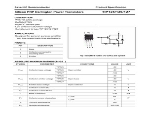
TIP125/126/127 DESCRIPTION *With TO-220C package *DARLNGTON *High DC current gain *Low collector saturation voltage *Complement to type TIP120/121/122 APPLICATIONS *Designed for general-purpose amplifier and low-speed switching applications PINNING PIN DESCRIPTION 1 Base 2 Collector;connected to mounting base 3 Emitter ABSOLUTE MAXIMUM RATINGS(Tc=25 ) SYMBOL PARAMETER CONDITIONS TIP125 VCBO VCEO Collector-base voltage Collector-emitter voltage TIP126 Open emitter Emitter-base voltage IC -80 TIP127 -100 TIP125 -60 TIP126 UNIT -60 Open base TIP127 VEBO VALUE -80 V V -100 Open collector -5 V Collector current-DC -5 A ICM Collector current-Pulse -8 A IB Base current-DC -120 mA PC Collector power dissipation TC=25 65 Ta=25 2 Tj Junction temperature 150 Tstg Storage temperature -65~150 W SavantIC Semiconductor Product Specification Silicon PNP Darlington Power Transistors TIP125/126/127 CHARACTERISTICS Tj=25 unless otherwise specified SYMBOL PARAMETER CONDITIONS <
 4 Pages, 123 KB, Original
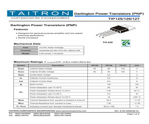
TIP125/126/127 Darlington Power Transistors (PNP) Features * Designed for general-purpose amplifier and low speed switching applications * RoHS Compliant TO-220 Mechanical Data Case: TO-220, Plastic Package Terminals: Weight: Solderable per MIL-STD-202, Method 208 0.08 ounces, 2.24 grams Maximum Ratings (T Ambient=25C unless noted otherwise) Symbol Description TIP125 TIP126 TIP127 Unit VCBO Collector-Base Voltage 60 80 100 V VCEO Collector-Emitter Voltage 60 80 100 V VEBO Emitter-Base Voltage 5.0 V Collector Current Continuous 5.0 A Collector Current Peak 8.0 A Base Current 120 mA Power Dissipation upto TC=25C 65 W Power Dissipation Derate above TC=25C 0.52 W/ C Power Dissipation upto TA=25C 2.0 W Power Dissipation Derate above TA=25C 16 mW/ C IC ICM IB PD RJA Thermal Resistance from Junction to Ambient in Free Air 62.5 C /W RJC Thermal Resistance from Junction to Case 1.92 C /W -65 to +150 C TJ, TSTG Operating Junction and Storage Temperature Range TAITRON COMPONENTS INCORPORATED ww
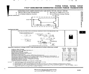
 4 Pages, 241 KB, Original
TIP125, TIP126, TIP127 P-N-P DARLINGTON-CONNECTED SILICON POWER TRANSISTORS devi DESIGNED FOR COMPLEMENTARY USE WITH TIP120, TIP 121, TIP 122 e 65 W at 25C Case Temperature e Minhge of 1000 at3V,3A 5A Rated Collector Current * 50 mJ Reverse Energy Rating ce schematic COLLECTOR BASE oT r----- EMITTER mechanical data THE COLLECTOR IS IN ELECTRICAL CONTACT WITH THE MOUNTING TAB MECHANICAL INTERCHANGEABILITY OF TIP125 PLASTIC PACKAGE WITH TO-06 GUTLINE 0.540 THiS PORTION OF LEADS, 9500 FREE OF FLASH JASE -= arte coecton ea > EMITTER - - = EE, 390 0.430 4 a210 ot k sil F 0 a6 oor 0018 LEADS 0375 3.199 ie TT os foie rt Et on ooss fF 0.695 0048 170 66 OLMENSIONS! 9210 0935 CASE TEMPERATURE 0790 9029 0030MIN f) MEASUREMENT POINT (2 PLACES) ry FE on 0161 6.090 ~ ansi OWA 0849 Mine Rao @ PLACES ALL DIMENSIONS ARE (N INCHES abso} NOTES: ute maximum ratings at 25C case temperature (unless otherwise noted) Collector-Base Voltage Collector-Emitter Voltage (See Note 1) Emitter-Base Voltage . . Cont
 4 Pages, 137 KB, Scan