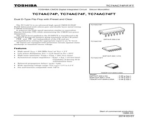
TC74AC74FT Dual D-Type Flip Flop with Preset and Clear The TC74AC74 is an advanced high speed CMOS D-FLIP FLOP fabricated with silicon gate and double-layer metal wiring C2MOS technology. It achieves the high speed operation similar to equivalent Bipolar Schottky TTL while maintaining the CMOS low power dissipation. The signal level applied to the D INPUT is transferred to Q OUTPUT during the positive going transition of the CK pulse. CLR and PR are independent of the CK and are accomplished by setting the appropriate input to an "L" level. All inputs are equipped with protection circuits against static discharge or transient excess voltage. TC74AC74P TC74AC74F Features * High speed: fmax = 200 MHz (typ.) at VCC = 5 V * Low power dissipation: ICC = 4 A (max) at Ta = 25C * High noise immunity: VNIH = VNIL = 28% VCC (min) * Symmetrical output impedance: |IOH| = IOL = 24 mA (min) * Capability of driving 50 transmission lines. tpHL Balanced propagation delays: tpLH - * Wide operating voltage range: V
 9 Pages, 226 KB, Original
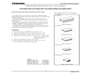
TC74AC74FT Dual D-Type Flip Flop with Preset and Clear Note: xxxFN (JEDEC SOP) is not available in Japan. The TC74AC74 is an advanced high speed CMOS D-FLIP FLOP fabricated with silicon gate and double-layer metal wiring C2MOS technology. It achieves the high speed operation similar to equivalent Bipolar Schottky TTL while maintaining the CMOS low power dissipation. The signal level applied to the D INPUT is transferred to Q OUTPUT during the positive going transition of the CK pulse. CLR and PR are independent of the CK and are accomplished by setting the appropriate input to an "L" level. All inputs are equipped with protection circuits against static discharge or transient excess voltage. TC74AC74P TC74AC74F Features * High speed: fmax = 200 MHz (typ.) at VCC = 5 V * Low power dissipation: ICC = 4 A (max) at Ta = 25C * High noise immunity: VNIH = VNIL = 28% VCC (min) * Symmetrical output impedance: |IOH| = IOL = 24 mA (min) * Capability of driving 50 transmission lines. tpHL Balanced propagati
 10 Pages, 229 KB, Original
TC74AC74FT Dual D-Type Flip Flop with Preset and Clear Note: xxxFN (JEDEC SOP) is not available in Japan. The TC74AC74 is an advanced high speed CMOS D-FLIP FLOP fabricated with silicon gate and double-layer metal wiring C2MOS technology. It achieves the high speed operation similar to equivalent Bipolar Schottky TTL while maintaining the CMOS low power dissipation. The signal level applied to the D INPUT is transferred to Q OUTPUT during the positive going transition of the CK pulse. CLR and PR are independent of the CK and are accomplished by setting the appropriate input to an "L" level. All inputs are equipped with protection circuits against static discharge or transient excess voltage. TC74AC74P TC74AC74F Features * High speed: fmax = 200 MHz (typ.) at VCC = 5 V * Low power dissipation: ICC = 4 A (max) at Ta = 25C * High noise immunity: VNIH = VNIL = 28% VCC (min) * Symmetrical output impedance: |IOH| = IOL = 24 mA (min) * Capability of driving 50 transmission lines. tpHL Balanced propagati
 10 Pages, 271 KB, Original
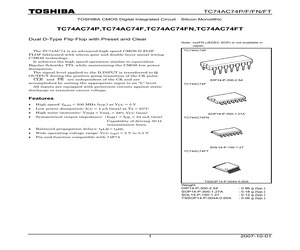
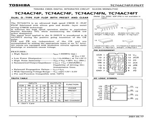
TC74AC74FT Dual D-Type Flip Flop with Preset and Clear TC74AC74 2 CMOS CMOS D CMOS TTL D Q "L" TC74AC74P TC74AC74F * : fmax = 200 MHz () (VCC = 5 V) * : ICC = 4 A () (Ta = 25C) * : VNIH = VNIL = 28% VCC () * * : |IOH| = IOL = 24 mA () : tpLH - tpHL * * 74F74 : VCC (opr) = 2~5.5 V TC74AC74FT DIP14-P-300-2.54 SOP14-P-300-1.27A TSSOP14-P-0044-0.65A 1 : 0.96 g () : 0.18 g () : 0.06 g () 2007-10-01 TC74AC74P/F/FT 1 1CLR 14 VCC 13 2CLR 12 2D 1D 2 1CK 3 1PR 4 11 2CK 1Q 5 10 2PR 1Q 6 9 2Q GND 7 8 2Q D Q CK Q CK Q D Q (4) (3) (2) (1) (10) (11) (12) (13) 1PR 1CK 1D 1CLR 2PR 2CK 2D 2CLR S (5) C1 1D R 1Q (6) 1Q (9) 2Q (8) 2Q (top view) Inputs Outputs Function CLR PR D CK Q Q L H X X L H Clear H L X X H L Preset X L L X H H H H L L H H H H H L H H X Qn Qn No Change X: Don't care CLR PR 1/13 4/10 6/8 D 2/12 5/9 Q Q CK 3/11 2 2007-10-01 TC74AC74P/F/FT ( 1) VCC -0.5~7.0 V VIN -0.5~VCC + 0.5 V VOUT -0.5~VCC + 0.5 V IIK 20 mA IOK 50 mA IOUT 50 mA ICC 100 mA / G N D PD 500 (DIP) ( 2)/180 (SOP/TSSOP) mW
 9 Pages, 298 KB, Original
TC74AC74FT Dual D-Type Flip Flop with Preset and Clear Note: xxxFN (JEDEC SOP) is not available in Japan. The TC74AC74 is an advanced high speed CMOS D-FLIP FLOP fabricated with silicon gate and double-layer metal wiring C2MOS technology. It achieves the high speed operation similar to equivalent Bipolar Schottky TTL while maintaining the CMOS low power dissipation. The signal level applied to the D INPUT is transferred to Q OUTPUT during the positive going transition of the CK pulse. CLR and PR are independent of the CK and are accomplished by setting the appropriate input to an "L" level. All inputs are equipped with protection circuits against static discharge or transient excess voltage. TC74AC74P TC74AC74F Features * High speed: fmax = 200 MHz (typ.) at VCC = 5 V * Low power dissipation: ICC = 4 A (max) at Ta = 25C * High noise immunity: VNIH = VNIL = 28% VCC (min) * Symmetrical output impedance: |IOH| = IOL = 24 mA (min) * Capability of driving 50 transmission lines. tpHL Balanced propagati
 11 Pages, 309 KB, Original
TC74AC74FT Dual D-Type Flip Flop with Preset and Clear Note: xxxFN (JEDEC SOP) is not available in Japan. The TC74AC74 is an advanced high speed CMOS D-FLIP FLOP fabricated with silicon gate and double-layer metal wiring C2MOS technology. It achieves the high speed operation similar to equivalent Bipolar Schottky TTL while maintaining the CMOS low power dissipation. The signal level applied to the D INPUT is transferred to Q OUTPUT during the positive going transition of the CK pulse. CLR and PR are independent of the CK and are accomplished by setting the appropriate input to an "L" level. All inputs are equipped with protection circuits against static discharge or transient excess voltage. TC74AC74P TC74AC74F Features * High speed: fmax = 200 MHz (typ.) at VCC = 5 V * Low power dissipation: ICC = 4 A (max) at Ta = 25C * High noise immunity: VNIH = VNIL = 28% VCC (min) * Symmetrical output impedance: |IOH| = IOL = 24 mA (min) * Capability of driving 50 transmission lines. Balanced propagation de
 11 Pages, 428 KB, Original
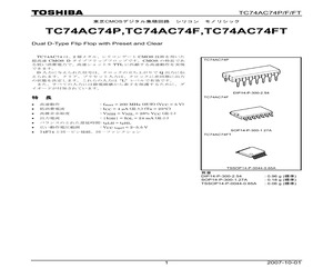
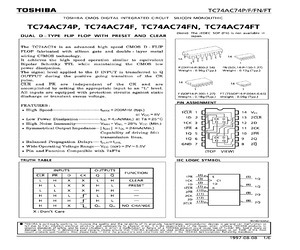
TC74AC74FT (Note) The JEDEC SOP (FN) is not available in DUAL D-TYPE FLIP FLOP WITH PRESET AND CLEAR Japan. The TC74AC74 is an advanced high speed CMOS D- FLIP FLOP fabricated with silicon gate and double - layer metal wiring C2MOS technology. It achieves the high speed operation similar to equivalent Bipolar Schottky TTL while maintaining the CMOS low power dissipation. P (DIP14-P-300-2.54) FN (SOL14-P-150-1.27) The signal level applied to the D INPUT is transferred to Q Weight: 0.969 (Typ.)_ Weight: 0.129 (Typ.) OUTPUT during the positive going transition of the CK pulse. CLR and PR are independent of the CK and are accomplished by setting the appropriate input to an L level. 1 1 All inputs are equipped with protection circuits against static F (SOP14-P-300-1.27) FT (TSSOP14-P-0044-0.65) discharge or transient excess voltage. Weight : 0.18g (Typ.) Weight : 0.06g (Typ.) PIN ASSIGNMENT FEATURES : High Speedssssesceescccsssesssecseesses fray = 200MHZ (typ. _ e High Spee MAX (typ.) aR 1 at Voc =5V
 7 Pages, 278 KB, Scan
C4S66F TC4S69F TC4S71F TC4S81F TC4SU11F TC4SU69F TC74AC00FN TC74AC00FT TC74AC02FN TC74AC02FT TC74AC04FN TC74AC04FT TC74AC04P TC74AC05FN TC74AC08FN TC74AC08FT TC74AC10FN TC74AC11FN TC74AC14FN TC74AC14FT TC74AC20FN TC74AC32FN TC74AC32FT TC74AC32P TC74AC74FN TC74AC74FT TC74AC74P TC74AC86FN TC74AC86FT TC74AC112FN TC74AC125FN TC74AC125FT TC74AC126FN TC74AC138FN TC74AC138FT TC74AC139FN TC74AC139FT TC74AC151FN TC74AC153FN TC74AC157FN TC74AC157FT TC74AC161FN TC74AC161FT TC74AC163FN TC74AC163FT TC74AC164FN TC74AC164FT TC74AC164P TC74AC166FN TC74AC174FN TC74AC174FT TC74AC175FN TC74AC175FT TC74AC240FT TC74AC244FT TC74AC245FT TC74AC257FN TC74AC258FN TC74AC273FT TC74AC280FN TC74AC283FN TC74AC367FN TC74AC367FT TC74AC373FT TC74AC374FT Page 14 14 14 14 14 14 14 14 14 14 14 19 19 19 19 19 19 19 19 19 19 15 15 15 15 15 15 15 15 15 15 15 15 15 15 15 15 15 15 15 15 15 15 15 15 15 15 15 15 15 15 15 15 15 15 15 15 15 15 15 15 15 15 15 15 15 15 15 16 16 16 16 16 16 16 16 16 16 16 16 Device TC74AC390FN TC74AC393FN TC74A
 80 Pages, 2176 KB, Original
TC74AC74FT (Note} The JEDEC SOP (FN) is not available in DUAL D-TYPE FLIP FLOP WITH PRESET AND CLEAR Japan. The TC74AC74 is an advanced high speed CMOS D - FLIP FLOP fabricated with silicon gate and double - layer metal wiring C2MOS technology. Ii achieves the high speed operation similar to equivalent Bipolar Schottky TTL while maintaining the CMOS low power dissipation. The signal level applied to the D INPUT is transferred to Q QUTPUT during the positive going transition of the CK pulse. P (DIP14-P-300-2.54) FN (SQOL14-P-150-1.27) Weight : 0.969 (Typ.) Weight: 0.129 (Typ.) CLR and PR are independent of the CK and are Xe eee accomplished by setting the appropriate input to an L level. 1 1 All inputs are equipped with protection circuits against static F(SOP14-P-300-1.27) FT {TSSOP14-P-0044-0.65) discharge or transient excess voltage. Weight : 0.18g(Typ.) Weight : 0.06g (Typ.) PIN ASSIGNMENT FEATURES : High Speedsessssscsssseseccssssssseseasenees faa = 200MHZ (typ. e High Spee MAX (typ.) ak 1 F
 6 Pages, 113 KB, Scan