uits, the high gain, high CMRR, and low TCVOS of the OP77 ensure high accuracy. The high gain and low TCVOS ensure accurate operation with inputs from microvolts to volts. In Figure 33, the signal always appears as a common-mode signal to the op amps. The OP77EZ CMRR of 1 V/V ensures errors of less than 2 ppm. 1k 1k +15V +15V 0.1F C1 30pF 0.1F 2 3 VIN D1 1N4148 7 2 D2 3 6 OP77E 7 OP77E VOUT 0 < VOUT < 10V 4 0.1F 2N4393 4 0.1F 6 R3 2k 00320-035 OP77 VIN R1 VIN > 0V IO = -15V -15V Figure 33. Precision Absolute Value Amplifier 15V + 2 2 2 10F REF-01 VO 4 REF-01 REF-01 6 VO 4 6 VO 6 4 100 OP77 VOUT 100 100 0.1F Figure 34. Low Noise Precision Reference Rev. G | Page 12 of 16 00320-036 VIN IRF520 VIN VIN IO = R1 VIN > 0V FULL SCALE OF 1V. IO = 1A/V 00320-033 IO 200 Data Sheet OP77 In Figure 35, CH must be of polystyrene, Teflon*, or polyethylene to minimize dielectric absorption and leakage. The droop rate is determined by the size of CH and the bias current of the AD820. Figure 34 relies upon low TCVO
 17 Pages, 379 KB, Original
uits, the high gain, high CMRR, and low TCVOS of the OP77 ensure high accuracy. The high gain and low TCVOS ensure accurate operation with inputs from microvolts to volts. In Figure 33, the signal always appears as a common-mode signal to the op amps. The OP77EZ CMRR of 1 V/V ensures errors of less than 2 ppm. 1k 1k +15V +15V 0.1F 2 3 VIN D1 1N4148 7 6 OP77E 2 D2 3 7 OP77E VOUT 0 < VOUT < 10V 4 0.1F 2N4393 4 0.1F 6 R3 2k 00320-035 C1 30pF 0.1F -15V -15V Figure 33. Precision Absolute Value Amplifier 15V + 10F 2 2 REF-01 VO 4 6 2 REF-01 VO 4 6 REF-01 VO 6 4 100 OP77 VOUT 100 100 0.1F Figure 34. Low Noise Precision Reference Rev. F | Page 12 of 16 00320-036 OP77 VIN VIN IO = R1 VIN > 0V FULL SCALE OF 1V. IO = 1A/V 00320-032 VIN OP77 00320-033 RL Data Sheet OP77 In Figure 35, CH must be of polystyrene, Teflon*, or polyethylene to minimize dielectric absorption and leakage. The droop rate is determined by the size of CH and the bias current of the AD820. Figure 34 relies upon low TCVOS of the OP77 and
 16 Pages, 386 KB, Original
16 18 18 20 20 20 12 12 12 12 12 15 18 18 18 18 36 80 80 80 80 80 140 140 120 120 132 132 132 80 80 80 80 80 118.06 120 120 120 120 76 0.9 0.9 0.9 0.9 0.9 1.14 1.14 2.5 2.5 0.38 0.38 0.38 3.2 3.2 3.2 3.2 3.2 0.9 2.4 2.4 2.4 2.4 5.5 OP07CPZ OP07CSZ OP07EPZ OP77EZ OP77FJZ OP200AZ OP200EZ OP200GPZ OP200GSZ OP400EY OP400GPZ OP400GSZ OP400HPZ OP400HS OP400HSZ PDIP-8 SOIC-8 PDIP-8 CDIP-8 TO-99-8 CDIP-8 CDIP-8 PDIP-8 SOIC-16 CDIP-14 PDIP-14 SOIC-16 PDIP-14 SOIC-16 SOIC-16 1 1 1 1 1 2 2 2 2 4 4 4 4 4 4 18 18 18 18 18 18 18 18 18 18 18 18 18 18 18 120 120 120 130 130 130 130 130 130 130 130 130 130 OP90GPZ OP90GSZ OP296GSZ OP296HRUZ-REEL AD8546ARMZ OP293ESZ OP293FSZ OP290GPZ OP496GSZ AD8548ARZ OP490GPZ AD8659ARZ AD8659ARZ-R7 OP490GSZ PDIP-8 SOIC-8 SOIC-8 TSSOP-8 MSOP-8 SOIC-8 SOIC-8 PDIP-8 SOIC-14 SOIC-14 PDIP-14 SOIC-14 SOIC-14 SOIC-16 1 1 2 2 2 2 2 2 4 4 4 4 4 4 36 36 5 5 18 18 18 36 5 18 18 18 18 28 OP196GSZ OP191GSZ OP193FSZ SOICSOIC-8 SOIC-8 1 1 1 OP497FPZ OP497FSZ OP497GPZ OP497GSZ PDIP-14 SOIC-16 P
 1 Pages, 232 KB, Original
uits, the high gain, high CMRR, and low TCVOS of the OP77 ensure high accuracy. The high gain and low TCVOS ensure accurate operation with inputs from microvolts to volts. In Figure 33, the signal always appears as a common-mode signal to the op amps. The OP77EZ CMRR of 1 V/V ensures errors of less than 2 ppm. 1k 1k +15V +15V 0.1F 2 3 VIN D1 1N4148 7 2 D2 3 6 OP77E 7 OP77E VOUT 0 < VOUT < 10V 4 0.1F 2N4393 4 0.1F 6 R3 2k 00320-035 C1 30pF 0.1F -15V -15V Figure 33. Precision Absolute Value Amplifier 15V + 2 2 2 10F REF-01 VO 4 REF-01 6 VO 4 REF-01 6 VO 6 4 100 OP77 VOUT 100 100 0.1F Figure 34. Low Noise Precision Reference Rev. E | Page 12 of 16 00320-036 OP77 IO = IRF520 VIN VIN 00320-033 IO VIN 200 OP77 Figure 34 relies upon low TCVOS of the OP77 and noise combined with very high CMRR to provide precision buffering of the averaged REF-01 voltage outputs. In Figure 35, CH must be of polystyrene, Teflon*, or polyethylene to minimize dielectric absorption and leakage. The droop rate is determined b
 16 Pages, 241 KB, Original
 for SO package. BONDING DIAGRAM 1. BALANCE 2. INVERTING INPUT 3. NONINVERTING INPUT 4. V6. OUTPUT 7. V+ 8. BALANCE DIE SIZE 0.093 0.057 inch, 5301 sq. mm (2.36 1.45 mm, 3.42 sq. mm) ORDERING GUIDE Package Options CERDIP* TO-99 8-Lead OP77EJ OP77FJ OP77AZ OP77EZ OP77FZ Operating Temperature Range MIL IND IND Not for new designs; obsolete April 2002. For Military processed devices, please refer to the Standard Microcircuit Drawing (SMD) available at www.dscc.dla.mil/programs/milspec/default.asp SMD Part Number ADI Equivalent 5962-87738012A 5962-8773802GA 5962-8773802PA OP77BRCMDA OP77AJMDA OP77AZMDA CAUTION ESD (electrostatic discharge) sensitive device. Electrostatic charges as high as 4000 V readily accumulate on the human body and test equipment and can discharge without detection. Although the OP77 features proprietary ESD protection circuitry, permanent damage may occur on devices subjected to high-energy electrostatic discharges. Therefore, proper ESD precautions are recommended to avoid per
 18 Pages, 356 KB, Original
and Figure 32, require the load to float between the power supply and the sink. The high gain and low TCVOS ensure accurate operation with inputs from microvolts to volts. In Figure 34, the signal always appears as a common-mode signal to the op amps. The OP77EZ CMRR of 1 V/V ensures errors of less than 2 ppm. In these circuits, the high gain, high CMRR, and low TCVOS of the OP77 ensure high accuracy. 1k 1k +15V +15V 0.1F C1 30pF 0.1F 2 3 VIN D1 1N4148 7 2 D2 3 6 OP77E 7 OP77E VOUT 0 < VOUT < 10V 4 0.1F 2N4393 4 0.1F 6 R3 2k -15V -15V Figure 34. Precision Absolute Value Amplifier 15V + 10F 2 2 REF-01 VO 4 1.6 In Figure 33, a simple bootstrapped voltage reference provides a precise 10 V that is virtually independent of changes in power supply voltage, ambient temperature, and output loading. The correct Zener operating current of exactly 2 mA is maintained by R1, a selected 5 ppm/C resistor, connected to the regulated output. Accuracy is primarily determined by three factors: the 5 ppm/C temperatu
 16 Pages, 261 KB, Original
 AD795JRZ AD8610ARZ AD8605ARTZ-REEL7 AD8628AUJZ-R2 AD8638ARJZ-R2 AD8638ARZ AD8663ARZ AD8671ARMZ AD8675ARZ ADA4004-1ARJZ-R2 OP07CPZ OP07CSZ OP07DNZ OP07EPZ OP177FPZ OP177GPZ AD8671ARZ ADA4004-1ARZ OP97EPZ OP97FPZ OP1177ARMZ-REEL OP1177ARZ OP177FSZ OP177GSZ OP77EZ OP97FSZ Stock No. 19M0981 19M8935 19M8977 59K6085 59K6941 19M8925 59K7002 89M5025 64M7591 61M4057 19P8315 84K9788 34P2945 59K8752 59K8753 19M1023 59K8756 59K8776 59K8777 19M0998 34P2947 59K8973 59K8974 19M8976 19M1025 19M8978 19M1026 05F8744 19M1037 1-24 3.81 3.15 5.07 3.81 4.14 3.11 7.32 6.59 8.71 7.84 1.65 1.53 3.23 3.00 4.54 3.58 3.31 2.31 3.13 2.79 2.75 2.27 3.10 2.77 5.79 5.38 1.57 1.42 1.57 1.42 1.30 1.15 3.88 3.47 5.72 5.11 2.01 1.82 2.75 2.46 4.69 3.53 7.77 6.99 2.88 2.57 2.38 2.21 2.38 1.70 5.72 5.11 2.01 1.82 10.81 9.83 2.88 2.57 0.3 20 0.15 0.4 0.4 3 5 5 13 0.3 60 60 5 1 41 11 20 4 2.7 2.7 0.04 0.7 22 0.15 5 0.1 11 4 0.4 0.15 0.15 0.15 0.1 0.08 0.075 0.005 0.005 0.75 0.065 0.02 0.325 0.1 0.085 80 5000 1000 0.1 0.25 0.4 0.075 0.
 375 Pages, 58008 KB, Original
uits, the high gain, high CMRR, and low TCVOS of the OP77 ensure high accuracy. The high gain and low TCVOS ensure accurate operation with inputs from microvolts to volts. In Figure 33, the signal always appears as a common-mode signal to the op amps. The OP77EZ CMRR of 1 V/V ensures errors of less than 2 ppm. 1k 1k +15V +15V 0.1F C1 30pF 0.1F 2 3 VIN D1 1N4148 7 2 D2 3 6 OP77E 7 OP77E VOUT 0 < VOUT < 10V 4 0.1F 2N4393 4 0.1F 6 R3 2k 00320-035 OP77 VIN R1 VIN > 0V IO = -15V -15V Figure 33. Precision Absolute Value Amplifier 15V + 2 2 2 10F REF-01 VO 4 REF-01 REF-01 6 VO 4 6 VO 6 4 100 OP77 VOUT 100 100 0.1F Figure 34. Low Noise Precision Reference Rev. G | Page 12 of 16 00320-036 VIN IRF520 VIN VIN IO = R1 VIN > 0V FULL SCALE OF 1V. IO = 1A/V 00320-033 IO 200 Data Sheet OP77 In Figure 35, CH must be of polystyrene, Teflon*, or polyethylene to minimize dielectric absorption and leakage. The droop rate is determined by the size of CH and the bias current of the AD820. Figure 34 relies upon low TCVO
 16 Pages, 353 KB, Original
3.59 NJM4560 0.38 NJM4560D 0.38 NJM4560L 2.23 NJM4560S 2.23 NJM4565D 1.09 NJM4565L 0.65 NJM4580L 1.10 NJM5532D 1.40 NJU7313AM*3.66 NM93C46N 2.19 NMC27C64Q200 3.40 NP7-12 19.95 NTP35N15 1.93 OP27EZ 15.78 OP400EY 17.41 OP400GS 8.04 OP491GS 5.93 OP497GP 6.70 OP77EZ 8.47 OPA111AM 20.34 OPA541AM102.20 OPA655U 16.20 PA3029 8.52 PA3029B 8.52 PAC006A 31.50 PAC006B 31.50 PAC007A 40.79 PAC008A 30.50 PAC010A 69.99 PAC011A 43.85 PAL001A 10.84 PAL003A 14.75 PAL005A 29.99 PAL006A 17.99 PAL007A 18.29 NET 30 Terms Order Toll Free 1-800-543-4330 Fax 1-800-765-6960 339 16 Order # (1-9) KIA7805API $0.40 KIA7809 1.62 KIA7812API 0.99 KIA7912PI 1.09 KIA8210H 5.98 KSA916 0.32 KSC1008 2.73 KSC1096 0.95 KSC1507 1.05 KSC1674 0.35 KSC1730 0.14 KSC2330 0.47 KSC2331 0.80 KSC815 0.06 KSC900 0.16 KSC945 0.08 KSP42 0.39 KSP44 0.33 KTA1266 1.03 L200CH 4.19 L295 4.66 L297 4.85 L298 11.81 L298N 11.81 L4960 8.14 L6203 16.62 L7805CV 0.87 L7809 1.67 L7812 4.06 L7812-220 0.43 L7812CV 0.43 L7815 1.52 L7815CV 1.58 LA1140 0.51 LA1185 2.3
 31 Pages, 2754 KB, Original
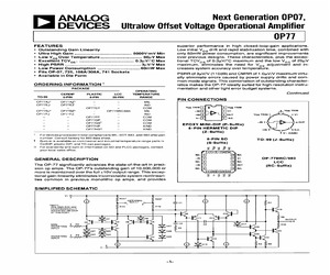
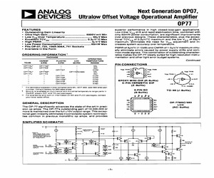
ow Power Consumption ...........::csscsssseseeeees Fits OP-07, 725, 108A/308A, 741 Sockets Available in Die Form oe @ @ @ # ORDERING INFORMATION PACKAGE OPERATING CERDIP PLASTIC Lcc TEMPERATURE TO-99 8-PIN 8-PIN 20-PIN RANGE OPT7AJ* OP77AZ* - - MIL OP77EJ OP77EZ - - IND - - OP77EP - COM OP77BU* OP77B2* - OP77BRC/883 MIL OP77FU OP77FZ - - IND - - OP77FP - COM - - OP77GP - COM - - op77Gs" - GOM - - OP77HP _ XIND - - OP77HStt - XIND For devices processed in total compliance to MIL-SDT-883, add /883 after part number. Consult factory for 883 data sheet. + Burn-in is available on commercial and industrial temperature range parts in CerDIP, plastic DIP, and TO-can packages. tt For availability and burn-in information on SO and PLCC packages, contact your local sales office. GENERAL DESCRIPTION The OP-77 significantly advances the state-of-the-art in preci- sion op amps. The OP-77's outstanding gain of 10,000,000 or more is maintained over the full +10V output range. This excep- tional gain-linearity el
 12 Pages, 418 KB, Scan
wer Consumption ............020..0.-ecesesseee 60mW Max * Fits OP-07, 725, 108A/308A, 741 Sockets * Available in Die Form ORDERING INFORMATION ' PACKAGE OPERATING CERDIP PLASTIC Lec TEMPERATURE TO-99 8-PIN 8-PIN 20-PIN RANGE OP77AJ* = OP77AZ* - MIL OP77EJ OP77EZ - IND ~ - OP77EP - COM OP77BJ* OP77BZ* - OP77BRC/883 MIL OP77FJ OP77FZ - - IND - - OP77FP - com - - oP77GP - CoM - ~ or77Gs" COM - OP77HP XIND - - OP77HS"" XIND * Far devices processed in total compliance to MIL-SDT-883, add /883 after part number. Consult factory for 889 data sheet. t Burn-in is available on commercial and industrial temperature range parts in CerDIP, plastic DIP, and TO-can packages. For ordering intormation, see 1990/91 Data Book, Section 2. For availability and burn-in information on SO and PLCC packages, contact your local sales office. GENERAL DESCRIPTION The OP-77 significantly advances the state-of-the-art in preci- sion op amps. The OP-77's outstanding gain of 10,000,000 or more is maintained over the full +10V o
 12 Pages, 370 KB, Scan
 for SO package. BONDING DIAGRAM 1. BALANCE 2. INVERTING INPUT 3. NONINVERTING INPUT 4. V6. OUTPUT 7. V+ 8. BALANCE DIE SIZE 0.093 0.057 inch, 5301 sq. mm (2.36 1.45 mm, 3.42 sq. mm) ORDERING GUIDE Package Options CERDIP* TO-99 8-Lead OP77EJ OP77FJ OP77AZ OP77EZ OP77FZ Operating Temperature Range MIL IND IND Not for new designs; obsolete April 2002. For Military processed devices, please refer to the Standard Microcircuit Drawing (SMD) available at www.dscc.dla.mil/programs/milspec/default.asp SMD Part Number ADI Equivalent 5962-87738012A 5962-8773802GA 5962-8773802PA OP77BRCMDA OP77AJMDA OP77AZMDA CAUTION ESD (electrostatic discharge) sensitive device. Electrostatic charges as high as 4000 V readily accumulate on the human body and test equipment and can discharge without detection. Although the OP77 features proprietary ESD protection circuitry, permanent damage may occur on devices subjected to high-energy electrostatic discharges. Therefore, proper ESD precautions are recommended to avoid per
 16 Pages, 290 KB, Original
ON ' istics makes the OP-77 ideally suited for high-resolution instru- PACKAGE mentation and other tight error budget systems. OPERATING CERDIP PLASTIC Lec TEMPERATURE Continued T0-99 8-PIN 8-PIN 20-PIN RANGE OP77AJ* OP77AZ* - _ MIL PIN CONNECTIONS OP77EJ OP77EZ - - IND _ - OP77EP - COM OP77Bs* OP77Bz* - OP77BRC/883 MIL 8 Vos TRIM OP77FJ OP77FZ - - IND - - OP77FP _ COM Vos TRIM 1 7 Vt - - OP77GP - COM - - op77Gs" - COM -IN2 6 OUT - - OP77HP - XIND EPOXY MINI-DIP (P-Suffix) - - oP77Hs" - XIND 8-PIN HERMETIC DIP Na - 7. + .C. * For devices processed in total compliance to MIL-SDT-883, add /883 after part (Z-Suftix) 4 V (CASE) number. Consult factory for 883 data sheet. 8-PIN so t Burn-in is available on commercial and industria! temperature range parts in (S-Suftix) TO-99 (J-Suffix) CerDIP, plastic DIP, and TO-can packages. For ordering information, see 1990/91 Data Book, Section 2. tt For availability and burn-in information on SO and PLCC packages, contact your local sales office. GENERAL DESCRIP
 12 Pages, 698 KB, Scan
.0 S S S S S S S S S S S S D D Q Q Q Q Q Precision Amplifiers Mfr.Os Type Vos Max. (V) VOS TC Max. (V/AC) Noise Vp-p 0.1-10 Hz Typ. GBW Typ. (MHz) Slew Rate (V/s Typ.) Ib nA Max. CMRR dB f=1 kHz Typ. Single Dual Quad OP177EZ OP177FP OP177GP OP177GS OP77EP OP77EZ OP77FJ OP77FP OP07CJ OP07CP OP07CS OP07DP OP07EJ OP07EP OP07EZ AD707JN OP77GP AD711KN AD711JN AD711JR AD712KN AD712JN AD712JR AD708BQ 25 25 25 25 25 25 60 60 75 75 75 75 75 75 75 90 100 500 1000 1000 1000 3000 3000 50 0.3 0.3 0.3 0.3 0.6 0.3 0.6 1.0 1.3 1.3 1.3 1.3 1.3 1.3 1.3 1.0 1.2 1.0 3.0 3.0 10.0 20.0 20.0 0.4 0.35 0.35 0.35 0.35 0.35 0.35 0.38 0.38 0.35 0.35 0.35 0.35 0.35 0.35 0.35 0.23 0.38 2.00 2.00 2.00 2.00 2.00 2.00 0.23 0.6 0.6 0.6 0.6 0.6 0.6 0.6 0.6 0.6 0.6 0.6 0.6 0.6 0.6 0.6 0.9 0.6 4.0 4.0 4.0 4.0 4.0 4.0 0.9 0.30 0.30 0.30 0.30 0.30 0.30 0.30 0.30 0.30 0.30 0.30 0.30 0.30 0.30 0.30 0.30 0.30 20.00 20.00 20.00 20.00 20.00 20.00 0.30 2.000 2.000 2.000 2.000 2.000 2.000 2.800 2.800 3.000 3.000 3.000 3.000 3.000 3.000 3.000
 1 Pages, 32 KB, Original
 Low Power Consumption ........cccseceserseeeees 60mW Max Fits OP-07, 725, 108A/308A, 741 Sockets * Available in Die Form ORDERING INFORMATION ' PACKAGE OPERATING CERDIP PLASTIC Lec TEMPERATURE TO-99 8-PIN 8-PIN 20-PIN RANGE OP77AJ" OP77Az" - - MIL OP77EJ OP77EZ - - IND - - OP77EP - COM OP77BJ* OP77B2* - OP77BRC/883 MIL OP77FJ OP77FZ - - IND - - OP77FP - COM - - OP77GP - COM - - op77Gs" - COM - - OP77HP - XIND - - OP77HStt - XIND For devices processed in total compliance to MIL-SDT-883, add /883 after part number. Consult factory for 883 data sheet. t Burn-in is available on commercial and industrial temperature range parts In CerDIP, plastic DIP, and TO-can packages. tt For availability and burn-in information on SO and PLCC packages, contact your local sales office. superior performance in high closed-loop-gain applications. Low initial V,,, drift and rapid stabilization time, combined with only 50mW power consumption, are significant improvements over previous designs. These characteristics, p
 12 Pages, 414 KB, Scan