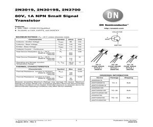
damage the device. Maximum Ratings are stress ratings only. Functional operation above the Recommended Operating Conditions is not implied. Extended exposure to stresses above the Recommended Operating Conditions may affect device reliability. JANTX2N3019 JANTXV2N3019 JAN2N3019S JANTX2N3019S JANTXV2N3019S JAN2N3700 JANTX2N3700 JANTXV2N3700 (c) Semiconductor Components Industries, LLC, 2012 August, 2012 - Rev. 2 1 Publication Order Number: 2N3019/D 2N3019, 2N3019S, 2N3700 ELECTRICAL CHARACTERISTICS (TA = 25C unless otherwise noted) Symbol Characteristic Min Max Unit 80 - - - 10 10 nAdc mAdc - 10 nAdc - 10 mAdc 50 90 100 50 15 300 - 300 300 - - - 0.2 0.5 - 1.1 5.0 20 80 400 - 12 - 60 - 4.0 - 400 - 30 OFF CHARACTERISTICS V(BR)CEO Collector -Emitter Breakdown Voltage (IC = 30 mAdc) Emitter-Base Cutoff Current (VEB = 5.0 Vdc) (VEB = 7.0 Vdc) IEBO Collector-Emitter Cutoff Current (VCE = 90 Vdc) ICEO Collector-Base Cutoff Current (VCB = 140 Vdc) ICBO Vdc ON CHARACTERISTICS (Note 1) DC Curre
 5 Pages, 113 KB, Original
JANSR2N2946A 251 20 X 251 20 JAN2N2218ALJANSR2N2946A JAN2N2218AL 391 30 X 391 30 JAN2N3019 JAN2N3019 251 20 X 251 20 JANTX2N2218AL JANTX2N2218AL 2N2218AL JANTX2N3019 391 30 X 391 30 JANTX2N3019 251 20 X X 391 251 20 JANTXV2N2218AL JANTXV2N2218AL 391 30 30 JANTXV2N3019 JANTXV2N3019 2N3019 391 30 30 251 20 X 391 251 20 JANS2N3019 JAN2N2219 JANS2N3019 JAN2N2219 391 391 30 X 30 JANSR2N3019 JANSR2N3019 251 20 X 251 20 JANTX2N2219JANTX2N2219 291 30 30 JAN2N3019S JAN2N3019S 251 20 X X 291 251 20 JANTXV2N2219 JANTXV2N2219 2N2219 291 30 30 JANTX2N3019S 251 20 X X 291 251 20 JANS2N2219 JANTX2N3019S JANS2N2219 291 291 30 X 30 JANTXV2N3019S JANTXV2N3019S 2N3019S 251 20 X 251 20 JANSR2N2219JANSR2N2219 291 30 X 291 30 JANS2N3019S JANS2N3019S 251 20 X 251 20 JAN2N2219A JAN2N2219A 291 30 X 291 30 JANSR2N3019S JANSR2N3019S 251 20 X 251 20 JANTX2N2219A JANTX2N2219A 2N2219A JAN2N3057A 391 30 X 391 30 JAN2N3057A 251 20 X 251 20 JANTXV2N2219A JANTXV2N2219A 391 30 X 391 30 JANTX2
 17 Pages, 6924 KB, Original
damage the device. Maximum Ratings are stress ratings only. Functional operation above the Recommended Operating Conditions is not implied. Extended exposure to stresses above the Recommended Operating Conditions may affect device reliability. JANTX2N3019 JANTXV2N3019 JAN2N3019S JANTX2N3019S JANTXV2N3019S JAN2N3700 JANTX2N3700 JANTXV2N3700 (c) Semiconductor Components Industries, LLC, 2012 August, 2012 - Rev. 2 1 Publication Order Number: 2N3019/D 2N3019, 2N3019S, 2N3700 ELECTRICAL CHARACTERISTICS (TA = 25C unless otherwise noted) Symbol Characteristic Min Max Unit 80 - - - 10 10 nAdc mAdc - 10 nAdc - 10 mAdc 50 90 100 50 15 300 - 300 300 - - - 0.2 0.5 - 1.1 5.0 20 80 400 - 12 - 60 - 4.0 - 400 - 30 OFF CHARACTERISTICS V(BR)CEO Collector -Emitter Breakdown Voltage (IC = 30 mAdc) Emitter-Base Cutoff Current (VEB = 5.0 Vdc) (VEB = 7.0 Vdc) IEBO Collector-Emitter Cutoff Current (VCE = 90 Vdc) ICEO Collector-Base Cutoff Current (VCB = 140 Vdc) ICBO Vdc ON CHARACTERISTICS (Note 1) DC Curre
 8 Pages, 275 KB, Original
damage the device. Maximum Ratings are stress ratings only. Functional operation above the Recommended Operating Conditions is not implied. Extended exposure to stresses above the Recommended Operating Conditions may affect device reliability. JANTX2N3019 JANTXV2N3019 JAN2N3019S JANTX2N3019S JANTXV2N3019S JAN2N3700 JANTX2N3700 JANTXV2N3700 (c) Semiconductor Components Industries, LLC, 2012 August, 2012 - Rev. 2 1 Publication Order Number: 2N3019/D 2N3019, 2N3019S, 2N3700 ELECTRICAL CHARACTERISTICS (TA = 25C unless otherwise noted) Symbol Characteristic Min Max Unit 80 - - - 10 10 nAdc mAdc - 10 nAdc - 10 mAdc 50 90 100 50 15 300 - 300 300 - - - 0.2 0.5 - 1.1 5.0 20 80 400 - 12 - 60 - 4.0 - 400 - 30 OFF CHARACTERISTICS V(BR)CEO Collector -Emitter Breakdown Voltage (IC = 30 mAdc) Emitter-Base Cutoff Current (VEB = 5.0 Vdc) (VEB = 7.0 Vdc) IEBO Collector-Emitter Cutoff Current (VCE = 90 Vdc) ICEO Collector-Base Cutoff Current (VCB = 140 Vdc) ICBO Vdc ON CHARACTERISTICS (Note 1) DC Curre
 4 Pages, 103 KB, Original
damage the device. Maximum Ratings are stress ratings only. Functional operation above the Recommended Operating Conditions is not implied. Extended exposure to stresses above the Recommended Operating Conditions may affect device reliability. JANTX2N3019 JANTXV2N3019 JAN2N3019S JANTX2N3019S JANTXV2N3019S JAN2N3700 JANTX2N3700 JANTXV2N3700 (c) Semiconductor Components Industries, LLC, 2012 August, 2012 - Rev. 2 1 Publication Order Number: 2N3019/D 2N3019, 2N3019S, 2N3700 ELECTRICAL CHARACTERISTICS (TA = 25C unless otherwise noted) Symbol Characteristic Min Max Unit 80 - - - 10 10 nAdc mAdc - 10 nAdc - 10 mAdc 50 90 100 50 15 300 - 300 300 - - - 0.2 0.5 - 1.1 5.0 20 80 400 - 12 - 60 - 4.0 - 400 - 30 OFF CHARACTERISTICS V(BR)CEO Collector -Emitter Breakdown Voltage (IC = 30 mAdc) Emitter-Base Cutoff Current (VEB = 5.0 Vdc) (VEB = 7.0 Vdc) IEBO Collector-Emitter Cutoff Current (VCE = 90 Vdc) ICEO Collector-Base Cutoff Current (VCB = 140 Vdc) ICBO Vdc ON CHARACTERISTICS (Note 1) DC Curre
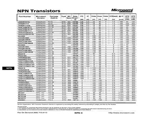
 6 Pages, 113 KB, Original
00 : JAN2N3019S Watertown | TO-39 STD 391 /19845/ 0.8 1 140 80 7 i 0.2 150 | 100 ' 300 | | JANTX2N3019 _- Watertown | TO-39 STD 39119843; 08 1 1 140 | 80 7 0.2 150 100 300 _JANTX2N3019S _. Watertown | TO-39 STD! 391 19846 08 1 140 | 80 7 0.2 150 100 300 | JANTXV2N3019 Watertown | TO-39 -STD! 391 19844 0.8 1. 140 | 80 7 0.2 150 100 300 | JANTXV2N3019S | Watertown | TO-39 STD: 391 19847 0.8 1 140 | 80 7 0.2 150 100 300 2N3501L ' Watertown: TO-5 STD: 366 19881 1 150 | 150 6 0.4 150 100 300 JAN2N3501 | Watertown | TO-39 STD 366 19878 1 150 | 150 6 0.4 150 100 300 JAN2N3501L ' Watertown . TO-5 STD. 366 19882: 1 150 | 150 6 0.4 150 100 300 _ JANTX2N3501 Watertown | TO-39 STD! 366 19879: 1 150 ; 150 6 0.4 150 100 300 JANTX2N3501L | Watertown TO-5 STD | 366 19883: 1 150 | 150 6 0.4 150 100 300 JANTXV2N3501_ | Watertown | TO-39 STD! 36619880 | 1 150 | 150 6 0.4 150 100: 300, JANTXV2N3501L | Watertown TO-5 STD 366 19884| 14 "150 | 150 6 | 04 150 100 | 300 | BC237 PPC, Inc. TO-92 STD | 24384 1
 1 Pages, 70 KB, Scan
et. PINs for types 2N3019 (1) PINs for types 2N3019S (1) PINs for types 2N3057A (1) PINs for types 2N3700 (1) PINs for types 2N3700UB (1) JAN2N3019 JAN2N3019S JAN2N3057A JAN2N3700 JAN2N3700UB JANTX2N3019 JANTX2N3019S JANTX2N3057A JANTX2N3700 JANTX2N3700UB JANTXV2N3019 JANTXV2N3019S JANTXV2N3057A JANTXV2N3700 JANTXV2N3700UB JANS2N3019 JANS2N3019S JANS2N3057A JANS2N3700 JANS2N3700UB JANTXVR2N3019 JANTXVR2N3019S JANTXVR2N3057A JANTXVR2N3700 JANTXVR2N3700UB JANTXVF2N3019 JANTXVF2N3019S JANTXVF2N3057A JANTXVF2N3700 JANTXVF2N3700UB JANS#2N3019 JANS#2N3019S JANS#2N3057A JANS#2N3700 JANS#2N3700UB (1) The number sign (#) represents one of eight RHA designators available (M, D, P, L, R, F, G, or H). * 6.6.1 PINs for unencapsulated devices (die). The following is a list of possible PINs for unencapsulated devices available on this specification sheet. PINs for types 2N3019 (1) PINs for types 2N3700 (1) JANHCA2N3019 JANHCA2N3700 JANHCB2N3700 JANHCC2N3700 JANKCA2N3019 JANKCA2N3700 JANKCB2N3700 JA
 40 Pages, 1140 KB, Original
damage the device. Maximum Ratings are stress ratings only. Functional operation above the Recommended Operating Conditions is not implied. Extended exposure to stresses above the Recommended Operating Conditions may affect device reliability. JANTX2N3019 JANTXV2N3019 JAN2N3019S JANTX2N3019S JANTXV2N3019S JAN2N3700 JANTX2N3700 JANTXV2N3700 (c) Semiconductor Components Industries, LLC, 2011 October, 2011 - Rev. 1 1 Publication Order Number: 2N3019/D 2N3019, 2N3019S, 2N3700 ELECTRICAL CHARACTERISTICS (TA = 25C unless otherwise noted) Characteristic Symbol Min Max Unit 80 - - - 10 10 nAdc mAdc - 10 nAdc - 10 mAdc 50 90 100 50 15 300 - 300 300 - - - 0.2 0.5 - 1.1 5.0 20 80 400 - 12 - 60 - 4.0 - 400 - 30 OFF CHARACTERISTICS Collector -Emitter Breakdown Voltage (IC = 30 mAdc) V(BR)CEO Emitter-Base Cutoff Current (VEB = 5.0 Vdc) (VEB = 7.0 Vdc) IEBO Collector-Emitter Cutoff Current (VCE = 90 Vdc) ICES Collector-Base Cutoff Current (VCB = 140 Vdc) ICBO Vdc ON CHARACTERISTICS (Note 1) DC Curr
 4 Pages, 101 KB, Original
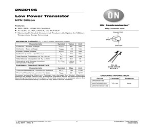
 = emitter, lead 2 = base, lead 3 = collector. T4-LDS-0185, Rev. 2 (121562) (c)2012 Microsemi Corporation Page 6 of 6 Mouser Electronics Authorized Distributor Click to View Pricing, Inventory, Delivery & Lifecycle Information: Microsemi: Jan2N3019 2N3019 JANTXV2N3019 JANS2N3019 Jantx2N3019
 7 Pages, 271 KB, Original
0-39 140 80 7 10 90 18 1A 10 0.2 11 150 | 12 100 400 50 12 50 200 0.1 10 05 500 90 10 10 100 = 300 150 10 50 200 500 10 JANTX2N3019 TO-39 140 80 7 10 90 | 50 200 0.1 10 0.20 14 150 | 12 100 400 50 12 90 10 10 0.50 500 100 300 150 10 50 200 500 10 15 1A 10 JANTXV2N3019 T0-39 140 80 7 10 90 | 50 200 0.1 10 0.2 Ww 150 | 12 100 400 50 12 90 10 10 0.5 500 100-300 150 10 50 200 500 10 15 1A 10 2N3020 TO-39 140 80 7 10 90 | 30 100 0.1 10 0.2 tA 150 | 12 100 50 12 40 120 150 10 05 500 15 1A 10 40 120 10 10 2N3053 TO-39 60 40 5 25 150 25 14 17 150 | 15 100 50 12 50-250 150 10 2N3107 TO-39 100 60 7 100 300 150 1 1 2 1A 20 350 50 12 35 0.1 10 0.25 ive 150 40 500 10 2N3108 TO-39 100 60 7 10 60 | 20 0.1 10 0.25 1 150 | 20 60 50 12 40 120 150 10 1 2 1A 25 500 10 2N3109 TO-39 80 40 7 10 60 | 35 0.1 10 0.25 14 150 | 25 70 50 12 100 300 150 1 1 2 1A 40 500 10 2N3110 TO-39 80 40 7 10 60 | 20 0.1 10 0.25 Ww 150 | 25 60 50 12 40 150 1 1 2 1A 25 500 10 2N3567 TO-105 80 40 5 50 40 | 40 30 1 0.25 150 | 20 60 200 50 14
 1 Pages, 26 KB, Scan
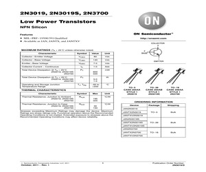
al operation above the Recommended Operating Conditions is not implied. Extended exposure to stresses above the Recommended Operating Conditions may affect device reliability. ORDERING INFORMATION Device Package Shipping TO-39 Bulk JAN2N3019S JANTX2N3019S JANTXV2N3019S (c) Semiconductor Components Industries, LLC, 2011 July, 2011 - Rev. 0 1 Publication Order Number: 2N3019S/D 2N3019S ELECTRICAL CHARACTERISTICS (TA = 25C unless otherwise noted) Symbol Characteristic Min Max 50 90 100 50 15 300 - 300 300 - - - 0.2 0.5 - 1.1 - 12 5.0 20 Unit ON CHARACTERISTICS hFE DC Current Gain (IC = 0.1 mAdc, VCE = 10 Vdc) (Note 1) (IC = 10 mAdc, VCE = 10 Vdc) (Note 1) (IC = 150 mAdc, VCE = 10 Vdc) (Note 1) (IC = 500 mAdc, VCE = 10 Vdc) (Note 1) (IC = 1.0 Adc, VCE = 10 Vdc) (Note 1) Collector -Emitter Saturation Voltage (Note 1) (IC = 150 mAdc, IB = 15 mAdc) (IC = 500 mAdc, IB = 50 mAdc) VCE(sat) Base -Emitter Saturation Voltage (Note 1) (IC = 150 mAdc, IB = 15 mAdc) VBE(sat) - Vdc Vdc SMALL-SIGNAL CHARACTERISTIC
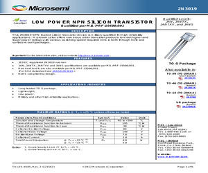
 3 Pages, 87 KB, Original
ional operation above the Recommended Operating Conditions is not implied. Extended exposure to stresses above the Recommended Operating Conditions may affect device reliability. ORDERING INFORMATION Device Package Shipping TO-5 Bulk JAN2N3019 JANTX2N3019 JANTXV2N3019 (c) Semiconductor Components Industries, LLC, 2011 July, 2011 - Rev. 0 1 Publication Order Number: 2N3019/D 2N3019 ELECTRICAL CHARACTERISTICS (TA = 25C unless otherwise noted) Symbol Characteristic Min Max 50 90 100 50 15 300 - 300 300 - - - 0.2 0.5 - 1.1 - 12 5.0 20 Unit ON CHARACTERISTICS hFE DC Current Gain (IC = 0.1 mAdc, VCE = 10 Vdc) (Note 1) (IC = 10 mAdc, VCE = 10 Vdc) (Note 1) (IC = 150 mAdc, VCE = 10 Vdc) (Note 1) (IC = 500 mAdc, VCE = 10 Vdc) (Note 1) (IC = 1.0 Adc, VCE = 10 Vdc) (Note 1) Collector -Emitter Saturation Voltage (Note 1) (IC = 150 mAdc, IB = 15 mAdc) (IC = 500 mAdc, IB = 50 mAdc) VCE(sat) Base -Emitter Saturation Voltage (Note 1) (IC = 150 mAdc, IB = 15 mAdc) VBE(sat) - Vdc Vdc SMALL-SIGNAL CHARACTERISTICS O
 3 Pages, 87 KB, Original