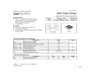
IRF7821PBF HEXFET(R) Power MOSFET Applications l High Frequency Point-of-Load Synchronous Buck Converter for Applications in Networking & Computing Systems. l Lead-Free Benefits l Very Low RDS(on) at 4.5V VGS l Low Gate Charge l Fully Characterized Avalanche Voltage and Current VDSS RDS(on) max Qg(typ.) 30V 9.1mW@VGS= 10V 9.3nC A A D S 1 8 S 2 7 D S 3 6 D G 4 5 D SO-8 Top View Absolute Maximum Ratings Parameter VDS Drain-to-Source Voltage Max. Units 30 V VGS Gate-to-Source Voltage 20 ID @ TA = 25C Continuous Drain Current, VGS @ 10V 13.6 ID @ TA = 70C Continuous Drain Current, VGS @ 10V 11 IDM Pulsed Drain Current 100 PD @TA = 25C Power Dissipation PD @TA = 70C Power Dissipation TJ Linear Derating Factor Operating Junction and TSTG Storage Temperature Range f f c A 2.5 W 1.6 0.02 -55 to + 155 W/C C Thermal Resistance Parameter RJL RJA g Junction-to-Ambient fg Junction-to-Drain Lead Typ. Max. Units --- 20 C/W --- 50 Notes through are on page 10 www.irf.com 1 5/6/04 IRF7821PBF Static @
 10 Pages, 267 KB, Original
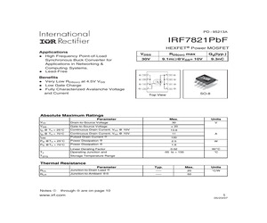
IRF7821PBF HEXFET(R) Power MOSFET Applications l High Frequency Point-of-Load Synchronous Buck Converter for Applications in Networking & Computing Systems. l Lead-Free Benefits l Very Low RDS(on) at 4.5V VGS l Low Gate Charge l Fully Characterized Avalanche Voltage and Current VDSS RDS(on) max Qg(typ.) 30V 9.1mW@VGS= 10V 9.3nC A A D S 1 8 S 2 7 D S 3 6 D G 4 5 D SO-8 Top View Absolute Maximum Ratings Parameter Max. Units 30 V VDS Drain-to-Source Voltage VGS Gate-to-Source Voltage Continuous Drain Current, VGS @ 10V 13.6 IDM Continuous Drain Current, VGS @ 10V Pulsed Drain Current 100 PD @TA = 25C Power Dissipation 2.5 PD @TA = 70C Power Dissipation TJ Linear Derating Factor Operating Junction and TSTG Storage Temperature Range ID @ TA = 25C ID @ TA = 70C f f 20 A 11 c W 1.6 0.02 -55 to + 155 W/C C Thermal Resistance Parameter RJL RJA g fg Junction-to-Ambient Junction-to-Drain Lead Notes through www.irf.com Typ. Max. Units --- 20 C/W --- 50 are on page 10 1 05/23/07 IRF7821PBF Static
 11 Pages, 290 KB, Original
IRF7821PBF HEXFET(R) Power MOSFET Applications l High Frequency Point-of-Load Synchronous Buck Converter for Applications in Networking & Computing Systems. l Lead-Free Benefits l Very Low RDS(on) at 4.5V VGS l Low Gate Charge l Fully Characterized Avalanche Voltage and Current VDSS RDS(on) max Qg(typ.) 30V 9.1mW@VGS= 10V 9.3nC A A D S 1 8 S 2 7 D S 3 6 D G 4 5 D SO-8 Top View Absolute Maximum Ratings Parameter Max. Units 30 V VDS Drain-to-Source Voltage VGS Gate-to-Source Voltage Continuous Drain Current, VGS @ 10V 13.6 IDM Continuous Drain Current, VGS @ 10V Pulsed Drain Current 100 PD @TA = 25C Power Dissipation 2.5 PD @TA = 70C Power Dissipation TJ Linear Derating Factor Operating Junction and TSTG Storage Temperature Range ID @ TA = 25C ID @ TA = 70C f f 20 A 11 c W 1.6 0.02 -55 to + 155 W/C C Thermal Resistance Parameter RJL RJA g fg Junction-to-Ambient Junction-to-Drain Lead Notes through www.irf.com Typ. Max. Units --- 20 C/W --- 50 are on page 10 1 05/23/07 IRF7821PBF Static
 10 Pages, 288 KB, Original
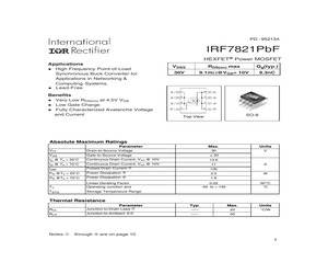
IRF7821PBF HEXFET(R) Power MOSFET Applications l High Frequency Point-of-Load Synchronous Buck Converter for Applications in Networking & Computing Systems. l Lead-Free Benefits l Very Low RDS(on) at 4.5V VGS l Low Gate Charge l Fully Characterized Avalanche Voltage and Current VDSS RDS(on) max Qg(typ.) 30V 9.1mW@VGS= 10V 9.3nC A A D S 1 8 S 2 7 D S 3 6 D G 4 5 D SO-8 Top View Absolute Maximum Ratings Parameter VDS Drain-to-Source Voltage Max. Units 30 V VGS Gate-to-Source Voltage 20 ID @ TA = 25C Continuous Drain Current, VGS @ 10V 13.6 ID @ TA = 70C Continuous Drain Current, VGS @ 10V 11 IDM Pulsed Drain Current 100 PD @TA = 25C Power Dissipation PD @TA = 70C Power Dissipation TJ Linear Derating Factor Operating Junction and TSTG Storage Temperature Range f f c A 2.5 W 1.6 0.02 -55 to + 155 W/C C Thermal Resistance Parameter RJL RJA g Junction-to-Ambient fg Junction-to-Drain Lead Typ. Max. Units --- 20 C/W --- 50 Notes through are on page 10 www.irf.com 1 11/3/04 IRF7821PBF Static
 10 Pages, 263 KB, Original
IRF7821PBF HEXFET(R) Power MOSFET Applications l High Frequency Point-of-Load Synchronous Buck Converter for Applications in Networking & Computing Systems. l Lead-Free Benefits l Very Low RDS(on) at 4.5V VGS l Low Gate Charge l Fully Characterized Avalanche Voltage and Current VDSS RDS(on) max Qg(typ.) 30V 9.1mW@VGS= 10V 9.3nC A A D S 1 8 S 2 7 D S 3 6 D G 4 5 D SO-8 Top View Absolute Maximum Ratings Parameter Max. Units 30 V VDS Drain-to-Source Voltage VGS Gate-to-Source Voltage Continuous Drain Current, VGS @ 10V 13.6 IDM Continuous Drain Current, VGS @ 10V Pulsed Drain Current 100 PD @TA = 25C Power Dissipation 2.5 PD @TA = 70C Power Dissipation TJ Linear Derating Factor Operating Junction and TSTG Storage Temperature Range ID @ TA = 25C ID @ TA = 70C f f 20 A 11 c W 1.6 0.02 -55 to + 155 W/C C Thermal Resistance Parameter RJL RJA g fg Junction-to-Ambient Junction-to-Drain Lead Notes through www.irf.com Typ. Max. Units --- 20 C/W --- 50 are on page 10 1 05/23/07 IRF7821PBF Static
 11 Pages, 290 KB, Original
lsed PD @ 25C 4 10 4.3 3.5 17 100 17 14 2.5 2.5 1.4 2 IR IR IR IR IRF1902PBF IRF7459TRPBF IRF7301PBF IRF7101PBF IRF7831PBF FDS8670 IRF7832ZPBF IRF7832PBF FDS8870 IRF7822.PBF PHK28NQ03LT IRF8113PBF IRF7463PBF IRF7809AVPBF IRF7477PBF SI4420DYPBF IRF7811WPBF IRF7821PBF IRF7828PBF STS12NF30L IRF7413PBF STS11NF30L IRF7811AVPBF STS9NF3LL IRF7403PBF IRF7807APBF IRF7805ZPBF IRF7413ZPBF IRF7805PBF IRF7807ZPBF IRF7416TRPBF IRF7807PBF IRF9410PBF IRF7201PBF STS6PF30L NDS8936 IRF7303PBF NDS9956A IRF9956PBF PSMN005-30K Mftrs. 30 30 30 30 30 30 30 30 30 30 30 30 30 30 30 30 30 30 30 30 30 30 30 30 30 30 30 30 30 30 30 30 30 30 30 30 0.0036 0.0037 3.8 0.004 0.0042 0.005 6.5mohm 0.0056 8mohm 0.0085 0.0085 0.009 0.009 0.0091 0.0095 0.009 0.01 0.0105 0.011 0.019 0.022 0.025 0.068 0.01 0.011 0.0138 0.02 0.025 0.03 0.03 0.03 0.03 0.05 0.08 0.1 4.4 21 21 21 20 18 18 23.7 17.2 14 14.5 14 12.5 14 13.6 13.6 12 12 11 10.8 9 6.7 8.3 16 13 13 11 10 8.3 7 7.3 6 6.7 4.9 3.7 3.5 20 170 105 160 160 90 150 60 135 110 100 110 50
 144 Pages, 26045 KB, Original
IRF7821PBF HEXFET(R) Power MOSFET Applications l High Frequency Point-of-Load Synchronous Buck Converter for Applications in Networking & Computing Systems. l Lead-Free Benefits l Very Low RDS(on) at 4.5V VGS l Low Gate Charge l Fully Characterized Avalanche Voltage and Current VDSS RDS(on) max Qg(typ.) 30V 9.1mW@VGS= 10V 9.3nC A A D S 1 8 S 2 7 D S 3 6 D G 4 5 D SO-8 Top View Absolute Maximum Ratings Parameter Max. Units 30 V VDS Drain-to-Source Voltage VGS Gate-to-Source Voltage Continuous Drain Current, VGS @ 10V 13.6 IDM Continuous Drain Current, VGS @ 10V Pulsed Drain Current 100 PD @TA = 25C Power Dissipation 2.5 PD @TA = 70C Power Dissipation TJ Linear Derating Factor Operating Junction and TSTG Storage Temperature Range ID @ TA = 25C ID @ TA = 70C f f 20 A 11 c W 1.6 0.02 -55 to + 155 W/C C Thermal Resistance Parameter RJL RJA g fg Junction-to-Ambient Junction-to-Drain Lead Typ. Max. Units --- 20 C/W --- 50 Notes through are on page 10 1 IRF7821PBF Static @ TJ = 25C (unless o
 4 Pages, 175 KB, Original
MIN_NECK_WIDTH=0.25 mm 1 MEM_ISENSE 6 NC 10% 16V X5R 402 1 10% 50V CERM 402 1 2 C7809 0.1uF PLACE C7804 NEAR U7801 PIN 7 MEM_ISENSE_R2 1 1 2 3 R7800 2.2 5% 1/16W MF-LF 402 Placement Note: 5% 1/16W MF-LF 402 2 MSOP SO-8 SMB C7807 + 2 THRML PAD 1 V+ 8 R1+ 3 IRF7821PBF 4 17 C7808 10% 16V X5R 402 Q7820 MIN_LINE_WIDTH=0.6 mm MIN_NECK_WIDTH=0.25 mm VCC 1 C7806 R1- MEM_ISENSE_R1_P 1V8S3_COMP_R 1 2 100 7 1 1% 1/10W MF-LF 603 =PP3V3_S3_PDCISENS 64 2 R7861 0.1UF 2 R7860 2.0K CRITICAL 8 VO 1% 1/16W MF-LF 2 402 R7802 20% 6.3V CERM1 603 LG 11 1V8S3_LG 1 1uF 10% 16V X5R 603 2.2UF CRITICAL 1 VIN 5 C7800 2 =PP1V8_S3_MEM_NB 100K GND_1V8S3_SGND 5 5% 1/16W MF-LF 402 2 12 PVCC 61 2 NO STUFF 1 2.2UF 1uF 5% 1/16W MF-LF 402 2 20% 16V POLY CASED2E-SM 2 3 C 63 60 45 23 C7831 1 C7830 1 MEM_ISENSE_R1_N 2 64 =PP1V8_S3_MEM_NB_SENSE 1 64 64 29 28 19 14 16 NO STUFF2 1% 1/16W MF-LF 402 C7803 0.0047uF 2 10% 25V CERM 402 1 2 3 SO-8 1 B R7822 2.0K 61 2 GND_1V8S3_SGND 1% 1/16W MF-LF 402 Vout = 0.6V * (1 + Ra / Rb) TABLE_ALT_HE
 79 Pages, 1535 KB, Original
1 2 C7842 330UF 20% 2.5V-ESR9V POLY CASE-D2E-LF R7801 5% 1/16W MF-LF 402 1 R7821 4.02K PP1V8_S3_R 1 22UF 20% 6.3V CERM-X5R 805 2 64 NO STUFF 0 1 330uF C7841 4 1 0.001uF 10% 50V CERM 402 SO-8 C7809 MIN_LINE_WIDTH=0.6 mm MIN_NECK_WIDTH=0.25 mm NO STUFF IRF7821PBF Placement Note: 5% 1/16W MF-LF 402 2 MSOP 1 2 3 R7800 2.2 5% 1/16W MF-LF 402 PGND 10 e r C7807 10% 16V X5R 402 Q7820 4 m il QFN 2 100 7 MEM_ISENSE_R1_P 1 U7800 R7860 2.0K 1% 1/10W MF-LF 603 =PP3V3_S3_PDCISENS 64 2 R7861 0.1UF 2 CRITICAL THRML PAD C7808 1 1/4W MF-LF 1206 MIN_LINE_WIDTH=0.6 mm MIN_NECK_WIDTH=0.25 mm ISL6269 17 1V8S3_COMP_R R7806 10% 16V X5R 603 0.005 1 1% 5 6 7 8 VCC 8 VO 1% 1/16W MF-LF 2 402 R7802 20% 6.3V CERM1 603 LG 11 1V8S3_LG 1 B 2 =PP1V8_S3_MEM_NB MEM_ISENSE_R1_N 1uF 2.2UF CRITICAL 1 VIN 5 5% 1/16W MF-LF 402 2 12 PVCC 61 2 NO STUFF 1 2.2UF 1uF 5% 1/16W MF-LF 402 2 2 1 C 1 20% 16V POLY CASED2E-SM C7831 1 1 1 C7804 64 29 28 19 14 16 3 NO STUFF C7806 1 33UF 1 1V8S3_VCC 1 C7830 =PP1V8_S3_MEM_NB_SENSE 2 64 63 60 45 23
 79 Pages, 1321 KB, Original
/50V 3 PC83 10U/16V_1206 2 PQ48A 2N7002DW 5 PR139 62_0805 1 23,29,30,34,38 SUS_ON 2 2 3 2 2 PR150 100K 4 1 1 1 6 5 2 1 PR174 62_0805 3 1 +5VRUN PQ46 FDC653N PR151 100K PR98 100K 1 +5VALW 3 2 1 2 15V 8 7 6 5 S 15V 4 G +5VALW 1 2 3 +5VALW +1_8VSUS_DDR2 PQ57 IRF7821PBF D 1 PR140 100K PC82 10U/16V_1206 PR108 100K C +1_5VSUS 4 2 PQ45B 2N7002DW 1 2 2 23,29,30,34,38 SUS_ON 1 2 3 1 1 +2_5VRUN_ALV 2 PQ45A 2N7002DW D +3VSUS 3 PR147 100K 2 2 PR148 100K Place near Alviso . +5VSUS For Alviso 6 5 2 1 1 1 PQ47 FDC653N 1 2 15V 2 1 +5VALW 3 +3VALW +3VRUN PQ43 FDC653N 6 5 2 1 PC81 10U/16V_1206 +VCCP MCH_VTT 1 PR126 100K 3 2 1 2 2 PR128 100K S 8 7 6 5 D PQ60 IRF7821PBF 15V 1 +5VALW B 4 G PQ33A 2N7002DW 1 1 +2_5VRUN_ALV +5VALW Discharge circuit for power-off +VCCP PR212 62_0805 PR141 62_0805 PR104 10K_0603 VTT_ON PR97 62_0805 2 PQ33B 2N7002DW 2 2 30 1 1 1 PR143 10K_0603 1 PR211 10K_0603 PC121 10U/16V_1206 PR127 NC_470K 2 +5VALW 4 +5VSUS PC125 4700P_0603/50V 6 +5VALW 1 5 1 1 3 1 B 2 3 1 4 2 2 6 1 1 HAI P
 43 Pages, 1285 KB, Original
 1 GENERIC SM_RES_2512, 0.7, 1W, 1%, TF, ROHS 29 R37 1 0.5 1W 1 GENERIC SM_RES_2512, 0.5, 1W, 1%, TF, ROHS 30 D1, D2 2 SSL_LXA3025IGC LUMEX SSL_LXA3025IGC_SMD-SSLLXA3025IGC,LED_3X2_5MM 31 D3, D4 2 BAT54S DIODES SM_SCHOTTKY_BAT54S-BAT54S, SOT23 32 Q2, Q4 2 IRF7821PBF IR 30V 13.6A N-Channel HEXFET Power MOSFET (Pb-free) 33 Q3, Q5 2 IRF7832PBF IR 30V 20A N-Channel HEXFET Power MOSFET (Pb-free) 34 Q1, Q6, Q10, Q12 4 2N7002-7-F FAIRCHILD 2N7002_SOT23-2N7002-7-F, SOT23 35 Q11, Q13 2 SUD50N03-07 VISHAY SUD50N03_07_TO252-SUD50N03-07,TO-252AA VALUE 4 VOLTAGE TOL. /POWER (%) MANUFACTURER DESCRIPTION AN1398.0 July 31, 2008 Application Note 1398 ISL62383LOEVAL1Z Evaluation Board Bill of Materials (Continued) NO. REFERENCE DESIGNATOR QTY 36 SW1, SW2 2 GT11MSCBE-T C&K GT11MSCKE_SMT-GT11MSCBE-T,GT13MSCKE 37 TP5, TP6, TP7, TP8, TP9, TP10, TP13,TP14, TP15 9 5002 KEYSTONE TEST_POINT_THOLE-5002,MTP500X 38 TP1, TP2, TP3, TP4, TP11, TP12 6 1514-2 KEYSTONE TEST_POINT_THOLE-1514-2, TP-150C100P 39 J1, J2, J3, J5 4 131-5
 14 Pages, 632 KB, Original
7 1W 1 GENERIC SM_RES_2512, 0.7, 1W, 1%, TF, ROHS 29 R37 1 0.5 1W 1 GENERIC SM_RES_2512, 0.5, 1W, 1%, TF, ROHS 30 D1 1 SSL_LXA3025IGC LUMEX SSL_LXA3025IGC_SMD-SSLLXA3025IGC,LED_3X2_5MM 31 D2, D3 2 BAT54S DIODES SM_SCHOTTKY_BAT54S-BAT54S, SOT23 32 Q2, Q4 2 IRF7821PBF IR 30V 13.6A N-Channel HEXFET Power MOSFET (Pb-free) 33 Q3, Q5 2 IRF7832PBF IR 30V 20A N-Channel HEXFET Power MOSFET (Pb-free) 34 Q1, Q10, Q12 3 2N7002-7-F FAIRCHILD 2N7002_SOT23-2N7002-7-F, SOT23 4 VALUE VOLTAGE/ TOL. POWER (%) MANUFACTURER DESCRIPTION AN1397.0 July 31, 2008 Application Note 1397 ISL62391LOEVAL1Z, ISL62392LOEVAL1Z Evaluation Board Bill of Materials ISL62391LOEVAL1Z and ISL62392LOEVAL1Z evaluation boards use the same PCB and schematic, thus the same bill of materials except for the controller U1. (Continued) NO REFERENCE DESIGNATOR QTY 35 Q11, Q13 2 SUD50N03-07 VISHAY SUD50N03_07_TO252-SUD50N03-07, TO252AA 36 SW1, SW2 2 GT11MSCBE-T C&K GT11MSCKE_SMT-GT11MSCBE-T, GT13MSCKE 37 TP5, TP6, TP7, TP8, TP9, TP10, TP13,TP14, T
 14 Pages, 608 KB, Original
 GENERIC SM_RES_2512, 0.7, 1W, 1%, TF, ROHS 31 R37 1 0.5 1W 1 GENERIC SM_RES_2512, 0.5, 1W, 1%, TF, ROHS 32 D1, D2 2 SSL_LXA3025IGC LUMEX SSL_LXA3025IGC_SMD-SSL-LXA3025IGC, LED_3x2_5MM 33 D3, D4 2 BAT54S DIODES SM_SCHOTTKY_BAT54S-BAT54S, SOT23 34 Q2, Q4 2 IRF7821PBF IR 30V 13.6A N-Channel HEXFET Power MOSFET (Pb-free) 4 VALUE VOLTAGE/ TOL. POWER (%) MANUFACTURER DESCRIPTION AN1396.0 July 31, 2008 Application Note 1396 ISL62381LOEVAL1Z, ISL62382LOEVAL1Z Evaluation Board Bill of Materials ISL62381LOEVAL1Z and ISL62382LOEVAL1Z evaluation boards use the same PCB and schematic, thus the same bill of materials except for the controller U1. (Continued) NO. REFERENCE DESIGNATOR QTY 35 Q3, Q5 2 IRF7832PBF IR 30V 20A N-Channel HEXFET Power MOSFET (Pb-FREE) 36 Q1, Q6, Q10, Q12 4 2N7002-7-F FAIRCHILD 2N7002_SOT23-2N7002-7-F,SOT23 37 Q11, Q13 2 SUD50N03-07 VISHAY SUD50N03_07_TO252-SUD50N03-07, TO-252AA 38 SW1, SW2 2 GT11MSCBE-T C&K GT11MSCKE_SMT-GT11MSCBE-T, GT13MSCKE 39 TP5, TP6, TP7, TP8, TP9, TP10, TP13, T
 13 Pages, 635 KB, Original
ISTOR, N-CHANNEL, 3LD, SOT-23, 60V, 115mA, ROHS DIODES INC. 2N7002-7-F-T DNP (Q5, Q10) TRANSISTOR-DUAL N-CHANNEL, 8P, SOIC, 30V, 7.5A, ROHS FAIRCHILD FDS6990AS 0 DNP (Q2, Q7) TRANSISTOR-MOS, N-CHANNEL, 8P, SOIC, 30V, 9.1m RDS, ROHS INTERNATIONAL RECTIFIER IRF7821PBF 2 Q1, Q6 TRANSISTOR-MOS, N-CHANNEL, 8P, SOIC, 30V, 9.1m RDS, INTERNATIONAL ROHS RECTIFIER IRF7821PBF 0 DNP (Q4, Q9) TRANSISTOR-MOS, N-CHANNEL, 8P, SOIC, 30V, 4.0m RDS, INTERNATIONAL ROHS RECTIFIER IRF7832PBF 2 Q3, Q8 TRANSISTOR-MOS, N-CHANNEL, 8P, SOIC, 30V, 4.0m RDS, INTERNATIONAL ROHS RECTIFIER IRF7832PBF 2 Q15, Q16 TRANSISTOR-MOS, N-CHANNEL, SMD, TO-252, 30V, 20A, ROHS VISHAY SUD50N03-07-E3 4 R9, R52, R53, R54 RES, SMD, 0603, 2, 1/10W, 1%, TF, ROHS YAGEO H2511-00020-1/10W1-T KOA H2511-00R00-1/10W-T 0 DNP (R12, R13, R57, R58) RESISTOR, SMD, 0603, 0, 1/10W, TF, ROHS AN1291 Rev 0.00 May 17, 2007 Page 5 of 14 ISL6228EVAL3Z Bill of Materials (Continued) QTY 10 REFERENCE DESCRIPTION R10, R11, R24, R25, R48, RESISTOR, SMD, 06
 14 Pages, 1137 KB, Original
2 1V8_VSSA NC_IRF7832TRPBF IRF7832TRPBF 2 VDDP2_1 VDDP2_2 PGND2_1 PGND2_2 4 G + PC371 2 VTT1 VTT2 PR99 NC_2.2_F 0402 PC312 PC97 NC_10P_50V_J_N 0402 1 0.1U_16V_Y_Y 0402 14 15 3 2 1 1V8_EN PQ78 D +1_8VSUS PVT modify PC311 NC_470U_2V_T EEFUD0D471LG D 1 2 3 1 IRF7821PBF 2 PQ77 EN/PSV 2 2 1 1V8_BST1 0402 2 PL20 1.0UH_11.5x10.4 PCMC104T-1R0MN 1 2 1 DL 1V8_DL S 470U_2V_T EEFUD0D471LG 1V8_LX 19 Place these CAPS close to FETs 7,11,13,14,61,62 4 G 2 22 PC307 0.1U_50V_K_B 0603 PQ31 1 LX VCCA PC306 10U_25V_M_B 1210 D 2 PR305 8.2K_F 1V8_ILIM 1 PC87 10U_25V_M_B 1210 1 ILIM 21 VTTS 37 PC84 10U_25V_M_B 1210 A63022 1_8V_DH 5 6 7 8 23 2 0402 1 2 3 DH 0_J 8 7 6 5 24 25 1 1V8_BST 1 BST THERMAL C 2 CLOSE_JUMP_40X50 18 Need to keep the 1_8V_DH& 1_8V_DL same length Width DH=40mils,DL=40mils M SC486IMLTRT N B 28,56,57,58,60,61,63 1 COMP 2 FB REF VSSA PC315 16 17 0.1U_16V_Y_Y 0402 2 1 PC314 10U_6.3V_Y_Y 0805 2 1 2 1 PC102 10U_6.3V_M 0805_X5R 2 1 PC103 10U_6.3V_M 0805_X5R 2 1 PC101 10U_6.3V_M 0805_X5R 2 1 PC100 10U_6.3V_M
 75 Pages, 1831 KB, Original