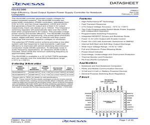
IRF7821PbF HEXFET(R) Power MOSFET Applications l High Frequency Point-of-Load Synchronous Buck Converter for Applications in Networking & Computing Systems. l Lead-Free Benefits l Very Low RDS(on) at 4.5V VGS l Low Gate Charge l Fully Characterized Avalanche Voltage and Current VDSS RDS(on) max Qg(typ.) 30V 9.1mW@VGS= 10V 9.3nC A A D S 1 8 S 2 7 D S 3 6 D G 4 5 D SO-8 Top View Absolute Maximum Ratings Parameter Max. Units 30 V VDS Drain-to-Source Voltage VGS Gate-to-Source Voltage Continuous Drain Current, VGS @ 10V 13.6 IDM Continuous Drain Current, VGS @ 10V Pulsed Drain Current 100 PD @TA = 25C Power Dissipation 2.5 PD @TA = 70C Power Dissipation TJ Linear Derating Factor Operating Junction and TSTG Storage Temperature Range ID @ TA = 25C ID @ TA = 70C f f 20 A 11 c W 1.6 0.02 -55 to + 155 W/C C Thermal Resistance Parameter RJL RJA g fg Junction-to-Ambient Junction-to-Drain Lead Notes through www.irf.com Typ. Max. Units --- 20 C/W --- 50 are on page 10 1 05/23/07 IRF7821PbF Static
 11 Pages, 290 KB, Original
C, ISL62383C Typical Application Circuits The below typical application circuits generate the 5V/8A and 3.3V/8A main supplies in a notebook computer. The input supply (VBAT) range is 5.5V to 25V VBAT 4x10F V IN BO O T1 BO O T2 0.22F 0.22F 4.7H 3 .3 V 330F IRF7821 UGATE1 UGATE2 PHASE1 PHASE2 LG ATE1 LGATE2 IRF7821 0.022F 14k 4.7H 5V 0.022F 330F 14k IRF7832 14k ISL62381 ISL62382 ISL62383 ISL62381C ISL62382C ISL62383C 750 OCSET1 45.3k IS E N 1 1200pF VOUT1 FB1 IRF7832 14k 750 OCSET2 68.1k IS E N 2 FB2 3 .3 V 10k LDO 3* 9.09k L D O 3 IN * 100k 17.4k 4.7F PGOOD1 LDO 3FB* 5V PGOOD2 10k 4.7F LDO5 LDO 3EN * FCCM FSET1 FSET2 VCC1 VCC2 1F LDO5 100k EN1 EN2 10 1F 1200pF VOUT2 PGND 0.01F 24.3k GND 19.6k 0.01F *ISL62381, ISL62382, ISL62381C, AND ISL62382C ONLY FIGURE 1. TYPICAL APPLICATION CIRCUIT WITH INDUCTOR DCR CURRENT SENSE VBAT BOOT1 4x10F 0.22F 0.001 330F 1k IRF7821 UGATE1 UGATE2 PHASE1 PHASE2 LG ATE1 LG ATE2 IRF7832 1k 750 1200pF BOOT2 IRF7821 4.7H 3 .3 V V IN 4.
 23 Pages, 517 KB, Original
 typical application circuits generate the 5V/8A and 3.3V/8A (system regulator), or 1.05V/15A and 1.5V/15A (chip set) supplies in a notebook computer. The input supply (VBAT) range is 5.5V to 25V. VBAT 4x10F BO OT1 V IN BOO T2 0.22F 0.22F 4.7H 3 .3 V 330F IRF7821 UGATE1 UGATE2 PHASE1 PHASE2 LGATE1 LG ATE2 IRF7821 5V 330F 14k 0.022F 0.022F 14k IRF7832 IRF7832 14k 4.7H 750 14k 45.3k 1200pF 750 OCSET2 OCSET1 IS E N 1 IS E N 2 VOUT1 VOUT2 68.1k 1200pF FB2 FB1 9.09k ISL62391, ISL62392 10k 100k PGOOD LDO3 4.7F PVCC EN1 EN2 LD O 3EN FCCM FSET1 FSET2 PVCC 1F VCC 1F PGND PAD 0.01F 24.3k 19.6k 0.01F FIGURE 1. TYPICAL SYSTEM REGULATOR APPLICATION CIRCUIT WITH INDUCTOR DCR CURRENT SENSE VBAT BO OT1 4x10F 0.22F 4.7H 3 .3 V 0.001 330F 1k V IN BO O T2 IRF7821 IRF7821 UG ATE1 UG ATE2 PHASE1 PHASE2 LGATE1 LG ATE2 OCSET1 OCSET2 4.7H 0.001 5V IRF7832 IRF7832 1k 0.22F 330F 1k 1k 750 750 1200pF 45.3k IS E N 1 IS E N 2 VO UT1 VOUT2 FB1 68.1k 1200pF FB2 9.09k ISL62391, ISL62392 10
 20 Pages, 492 KB, Original
381C, ISL62382C, ISL62383C Typical Application Circuits The below typical application circuits generate the 5V/8A and 3.3V/8A main supplies in a notebook computer. The input supply (VBAT) range is 5.5V to 25V VBAT 4x10F 4.7H 3 .3 V 330F V IN BO O T1 0.22F IRF7821 BO O T2 UGATE1 UGATE2 PHASE1 PHASE2 LG ATE1 LGATE2 0.22F IRF7821 0.022F 14k IRF7832 ISL62381 ISL62382 ISL62383 ISL62381C ISL62382C ISL62383C OCSET1 45.3k IS E N 1 1200pF VOUT1 10k FB1 3 .3 V LDO 3* 17.4k 4.7F 0.022F 330F LDO5 68.1k IS E N 2 1200pF FB2 9.09k 100k LDO5 100k EN1 EN2 LDO 3EN * FCCM FSET1 FSET2 VCC1 VCC2 1F 750 VOUT2 PGOOD1 10 1F 14k OCSET2 PGOOD2 10k 4.7F IRF7832 L D O 3 IN * LDO 3FB* 5V 5V 14k 14k 750 4.7H PGND 19.6k *ISL62381, ISL62382, ISL62381C, AND ISL62382C ONLY 0.01F 24.3k GND 0.01F FIGURE 1. TYPICAL APPLICATION CIRCUIT WITH INDUCTOR DCR CURRENT SENSE VBAT BOOT1 4x10F 0.22F 4.7H 3 .3 V 0.001 330F 1k 750 IRF7821 UGATE1 UGATE2 PHASE1 PHASE2 LG ATE1 LG ATE2 IS E N 1 45.3k VOUT1 FB1 3 .3 V 4.7F 5
 24 Pages, 1213 KB, Original
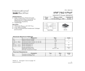
IRF7821 HEXFET(R) Power MOSFET Applications l High Frequency Point-of-Load Synchronous Buck Converter for Applications in Networking & Computing Systems. VDSS RDS(on) max Qg(typ.) 30V 9.1mW@VGS= 10V 9.3nC 1 8 S 2 7 S 3 6 4 5 S Benefits l Very Low RDS(on) at 4.5V VGS l Ultra-Low Gate Impedance l Fully Characterized Avalanche Voltage and Current G A A D D D D SO-8 Top View Absolute Maximum Ratings Max. Units VDS Drain-to-Source Voltage Parameter 30 V VGS Gate-to-Source Voltage 20 ID @ TA = 25C Continuous Drain Current, VGS @ 10V 13.6 ID @ TA = 70C Continuous Drain Current, VGS @ 10V 11 IDM Pulsed Drain Current 100 f f c PD @TA = 25C Power Dissipation PD @TA = 70C Power Dissipation TJ Linear Derating Factor Operating Junction and TSTG Storage Temperature Range A 2.5 W 1.6 0.02 -55 to + 150 W/C C Thermal Resistance Parameter RJL RJA Junction-to-Drain Lead Junction-to-Ambient f Typ. Max. Units --- 20 C/W --- 50 Notes through are on page 10 www.irf.com 1 2/25/03 IRF7821 Static @ TJ = 25C (
 10 Pages, 204 KB, Original
381C, ISL62382C, ISL62383C Typical Application Circuits The below typical application circuits generate the 5V/8A and 3.3V/8A main supplies in a notebook computer. The input supply (VBAT) range is 5.5V to 25V VBAT 4x10F 4.7H 3 .3 V 330F V IN BO O T1 0.22F IRF7821 BO O T2 UGATE1 UGATE2 PHASE1 PHASE2 LG ATE1 LGATE2 0.22F IRF7821 0.022F 14k IRF7832 ISL62381 ISL62382 ISL62383 ISL62381C ISL62382C ISL62383C OCSET1 45.3k IS E N 1 1200pF VOUT1 10k FB1 3 .3 V LDO 3* 17.4k 4.7F 0.022F 330F LDO5 68.1k IS E N 2 1200pF FB2 9.09k 100k LDO5 100k EN1 EN2 LDO 3EN * FCCM FSET1 FSET2 VCC1 VCC2 1F 750 VOUT2 PGOOD1 10 1F 14k OCSET2 PGOOD2 10k 4.7F IRF7832 L D O 3 IN * LDO 3FB* 5V 5V 14k 14k 750 4.7H PGND 19.6k *ISL62381, ISL62382, ISL62381C, AND ISL62382C ONLY 0.01F 24.3k GND 0.01F FIGURE 1. TYPICAL APPLICATION CIRCUIT WITH INDUCTOR DCR CURRENT SENSE VBAT BOOT1 4x10F 0.22F 4.7H 3 .3 V 0.001 330F 1k 750 IRF7821 UGATE1 UGATE2 PHASE1 PHASE2 LG ATE1 LG ATE2 IS E N 1 45.3k VOUT1 FB1 3 .3 V 4.7F 5
 25 Pages, 1104 KB, Original
0.00 February 4, 2009 Page 4 of 20 ISL62386 Typical Application Circuits The following typical application circuits generate the 5V/8A and 3.3V/8A main supplies in a notebook computer. The input supply (VBAT) range is 5.5V to 25V. VBAT 4x10F BO O T1 0.22F IRF7821 4.7H 3 .3 V 330F V IN BOOT2 UGATE1 UG ATE2 PHASE1 PHASE2 LG ATE1 LG ATE2 0.22F IRF7821 0.022F 14k 5V 0.022F 330F 14k IRF7832 IRF7832 ISL62386 14k 750 4.7H 45.3k VO UT1 68.1k 1200pF VOUT2 FB1 10k 750 IS E N 2 IS E N 1 1200pF 14k OCSET2 OCSET1 FB2 9.09k AGND1 AGND2 3 .3 V LDO3 4.7F 5V PGOOD LDO5 4.7F LD O 3EN FCCM FSET1 FSET2 VCC 1F LDO5 100k EN1 EN2 PGND 0.01F 24.3k 19.6k 0.01F A G N D 1 /2 AGND2 AGND1 FIGURE 1. TYPICAL APPLICATION CIRCUIT WITH INDUCTOR DCR CURRENT SENSE VBAT BOOT1 4x10F 4.7H 3 .3 V 0.001 330F V IN BOOT2 IRF7821 IRF7821 0.22F 1k UG ATE1 UGATE2 PHASE1 PHASE2 LG ATE1 LGATE2 IRF7832 1k 0.22F 4.7H 5V 0.001 330F IRF7832 1k 1k ISL62386 750 1200pF OCSET1 45.3k IS E N 1 IS E N 2 VO UT1 VOUT2
 21 Pages, 940 KB, Original
IRF7821PbF HEXFET(R) Power MOSFET Applications l High Frequency Point-of-Load Synchronous Buck Converter for Applications in Networking & Computing Systems. l Lead-Free Benefits l Very Low RDS(on) at 4.5V VGS l Low Gate Charge l Fully Characterized Avalanche Voltage and Current VDSS RDS(on) max Qg(typ.) 30V 9.1mW@VGS= 10V 9.3nC A A D S 1 8 S 2 7 D S 3 6 D G 4 5 D SO-8 Top View Absolute Maximum Ratings Parameter Max. Units 30 V VDS Drain-to-Source Voltage VGS Gate-to-Source Voltage Continuous Drain Current, VGS @ 10V 13.6 IDM Continuous Drain Current, VGS @ 10V Pulsed Drain Current 100 PD @TA = 25C Power Dissipation 2.5 PD @TA = 70C Power Dissipation TJ Linear Derating Factor Operating Junction and TSTG Storage Temperature Range ID @ TA = 25C ID @ TA = 70C f f 20 A 11 c W 1.6 0.02 -55 to + 155 W/C C Thermal Resistance Parameter RJL RJA g fg Junction-to-Ambient Junction-to-Drain Lead Notes through www.irf.com Typ. Max. Units --- 20 C/W --- 50 are on page 10 1 05/23/07 IRF7821PbF Static
 11 Pages, 290 KB, Original
0.00 February 4, 2009 Page 4 of 20 ISL62386 Typical Application Circuits The following typical application circuits generate the 5V/8A and 3.3V/8A main supplies in a notebook computer. The input supply (VBAT) range is 5.5V to 25V. VBAT 4x10F BO O T1 0.22F IRF7821 4.7H 3 .3 V 330F V IN BOOT2 UGATE1 UG ATE2 PHASE1 PHASE2 LG ATE1 LG ATE2 0.22F IRF7821 0.022F 14k 5V 0.022F 330F 14k IRF7832 IRF7832 ISL62386 14k 750 4.7H 45.3k VO UT1 68.1k 1200pF VOUT2 FB1 10k 750 IS E N 2 IS E N 1 1200pF 14k OCSET2 OCSET1 FB2 9.09k AGND1 AGND2 3 .3 V LDO3 4.7F 5V PGOOD LDO5 4.7F LD O 3EN FCCM FSET1 FSET2 VCC 1F LDO5 100k EN1 EN2 PGND 0.01F 24.3k 19.6k 0.01F A G N D 1 /2 AGND2 AGND1 FIGURE 1. TYPICAL APPLICATION CIRCUIT WITH INDUCTOR DCR CURRENT SENSE VBAT BOOT1 4x10F 4.7H 3 .3 V 0.001 330F V IN BOOT2 IRF7821 IRF7821 0.22F 1k UG ATE1 UGATE2 PHASE1 PHASE2 LG ATE1 LGATE2 IRF7832 1k 0.22F 4.7H 5V 0.001 330F IRF7832 1k 1k ISL62386 750 1200pF OCSET1 45.3k IS E N 1 IS E N 2 VO UT1 VOUT2
 21 Pages, 940 KB, Original
IRF7821PbF HEXFET(R) Power MOSFET Applications l High Frequency Point-of-Load Synchronous Buck Converter for Applications in Networking & Computing Systems. l Lead-Free Benefits l Very Low RDS(on) at 4.5V VGS l Low Gate Charge l Fully Characterized Avalanche Voltage and Current VDSS RDS(on) max Qg(typ.) 30V 9.1mW@VGS= 10V 9.3nC A A D S 1 8 S 2 7 D S 3 6 D G 4 5 D SO-8 Top View Absolute Maximum Ratings Parameter Max. Units 30 V VDS Drain-to-Source Voltage VGS Gate-to-Source Voltage Continuous Drain Current, VGS @ 10V 13.6 IDM Continuous Drain Current, VGS @ 10V Pulsed Drain Current 100 PD @TA = 25C Power Dissipation 2.5 PD @TA = 70C Power Dissipation TJ Linear Derating Factor Operating Junction and TSTG Storage Temperature Range ID @ TA = 25C ID @ TA = 70C f f 20 A 11 c W 1.6 0.02 -55 to + 155 W/C C Thermal Resistance Parameter RJL RJA g fg Junction-to-Ambient Junction-to-Drain Lead Notes through www.irf.com Typ. Max. Units --- 20 C/W --- 50 are on page 10 1 05/23/07 IRF7821PbF Static
 10 Pages, 288 KB, Original
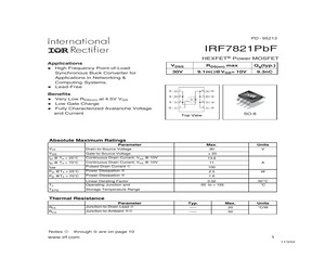
IRF7821PbF HEXFET(R) Power MOSFET Applications l High Frequency Point-of-Load Synchronous Buck Converter for Applications in Networking & Computing Systems. l Lead-Free Benefits l Very Low RDS(on) at 4.5V VGS l Low Gate Charge l Fully Characterized Avalanche Voltage and Current VDSS RDS(on) max Qg(typ.) 30V 9.1mW@VGS= 10V 9.3nC A A D S 1 8 S 2 7 D S 3 6 D G 4 5 D SO-8 Top View Absolute Maximum Ratings Parameter VDS Drain-to-Source Voltage Max. Units 30 V VGS Gate-to-Source Voltage 20 ID @ TA = 25C Continuous Drain Current, VGS @ 10V 13.6 ID @ TA = 70C Continuous Drain Current, VGS @ 10V 11 IDM Pulsed Drain Current 100 PD @TA = 25C Power Dissipation PD @TA = 70C Power Dissipation TJ Linear Derating Factor Operating Junction and TSTG Storage Temperature Range f f c A 2.5 W 1.6 0.02 -55 to + 155 W/C C Thermal Resistance Parameter RJL RJA g Junction-to-Ambient fg Junction-to-Drain Lead Typ. Max. Units --- 20 C/W --- 50 Notes through are on page 10 www.irf.com 1 11/3/04 IRF7821PbF Static
 10 Pages, 263 KB, Original
IRF7821UPbF HEXFET(R) Power MOSFET Applications l High Frequency Point-of-Load Synchronous Buck Converter for Applications in Networking & Computing Systems. l Lead-Free Benefits l Very Low RDS(on) at 4.5V VGS l Low Gate Charge l Fully Characterized Avalanche Voltage and Current VDSS RDS(on) max Qg(typ.) 30V 9.1mW@VGS= 10V 9.3nC A A D S 1 8 S 2 7 D S 3 6 D G 4 5 D SO-8 Top View Absolute Maximum Ratings Parameter Max. Units 30 V VDS Drain-to-Source Voltage VGS Gate-to-Source Voltage Continuous Drain Current, VGS @ 10V 13.6 IDM Continuous Drain Current, VGS @ 10V Pulsed Drain Current 100 PD @TA = 25C Power Dissipation 2.5 PD @TA = 70C Power Dissipation TJ Linear Derating Factor Operating Junction and TSTG Storage Temperature Range ID @ TA = 25C ID @ TA = 70C f f 20 A 11 c W 1.6 0.02 -55 to + 155 W/C C Thermal Resistance Parameter RJL RJA g fg Junction-to-Ambient Junction-to-Drain Lead Typ. Max. Units --- 20 C/W --- 50 Notes through are on page 10 www.irf.com 1 09/14/06 IRF7821UPbF Stat
 10 Pages, 261 KB, Original
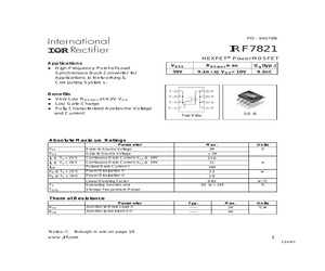
IRF7821 HEXFET(R) Power MOSFET Applications l High Frequency Point-of-Load Synchronous Buck Converter for Applications in Networking & Computing Systems. VDSS RDS(on) max Qg(typ.) 30V 9.1mW@VGS= 10V 9.3nC 1 8 S 2 7 S 3 6 4 5 S Benefits l Very Low RDS(on) at 4.5V VGS l Low Gate Charge l Fully Characterized Avalanche Voltage and Current G A A D D D D SO-8 Top View Absolute Maximum Ratings Parameter VDS Drain-to-Source Voltage Max. Units 30 V VGS Gate-to-Source Voltage 20 ID @ TA = 25C Continuous Drain Current, VGS @ 10V 13.6 ID @ TA = 70C Continuous Drain Current, VGS @ 10V 11 IDM Pulsed Drain Current 100 PD @TA = 25C Power Dissipation PD @TA = 70C Power Dissipation TJ Linear Derating Factor Operating Junction and TSTG Storage Temperature Range f f c A 2.5 W 1.6 0.02 -55 to + 155 W/C C Thermal Resistance Parameter RJL RJA g Junction-to-Ambient fg Junction-to-Drain Lead Typ. Max. Units --- 20 C/W --- 50 Notes through are on page 10 www.irf.com 1 1/14/03 IRF7821 Static @ TJ = 25C (unless
 10 Pages, 208 KB, Original
0.00 February 4, 2009 Page 4 of 20 ISL62386 Typical Application Circuits The following typical application circuits generate the 5V/8A and 3.3V/8A main supplies in a notebook computer. The input supply (VBAT) range is 5.5V to 25V. VBAT 4x10F BO O T1 0.22F IRF7821 4.7H 3 .3 V 330F V IN BOOT2 UGATE1 UG ATE2 PHASE1 PHASE2 LG ATE1 LG ATE2 0.22F IRF7821 0.022F 14k 5V 0.022F 330F 14k IRF7832 IRF7832 ISL62386 14k 750 4.7H 45.3k VO UT1 68.1k 1200pF VOUT2 FB1 10k 750 IS E N 2 IS E N 1 1200pF 14k OCSET2 OCSET1 FB2 9.09k AGND1 AGND2 3 .3 V LDO3 4.7F 5V PGOOD LDO5 4.7F LD O 3EN FCCM FSET1 FSET2 VCC 1F LDO5 100k EN1 EN2 PGND 0.01F 24.3k 19.6k 0.01F A G N D 1 /2 AGND2 AGND1 FIGURE 1. TYPICAL APPLICATION CIRCUIT WITH INDUCTOR DCR CURRENT SENSE VBAT BOOT1 4x10F 4.7H 3 .3 V 0.001 330F V IN BOOT2 IRF7821 IRF7821 0.22F 1k UG ATE1 UGATE2 PHASE1 PHASE2 LG ATE1 LGATE2 IRF7832 1k 0.22F 4.7H 5V 0.001 330F IRF7832 1k 1k ISL62386 750 1200pF OCSET1 45.3k IS E N 1 IS E N 2 VO UT1 VOUT2
 20 Pages, 952 KB, Original
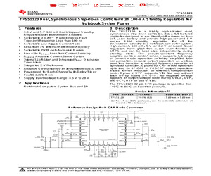
he end of the datasheet. Reference Design for D-CAP Mode Converter V5FILT VBAT EN_2 L2 2.2 H 2 1 COMP1 VO1 R11 100 k SKIPSEL 32 11 PGOOD2 PGOOD1 30 TPS51120RHB (QFN-32) P_GOOD1 GND VBAT EN1 29 EN_1 13 VBST2 VBST1 28 C11 0.1 F 14 DRVH2 DRVH1 27 C10 20 F Q1 IRF7821 L1 4.7 H + + PowerPAD CS1 PGND1 17 VIN DRVL2 VREG5 16 V5FILT Q4 IRF7832 LL1 26 VREG3 C2A 150 F 15 LL2 CS2 C2B 150 F VO2_GND 3 TONSEL 31 12 EN2 C21 0.1 F 4 10 EN3 PGND2 VO2 3.3V/6A Q3 IRF7821 5 VFB1 EN5 EN_LDO3 C10 20 F 6 GND 9 7 VFB2 EN_LDO5 P_GOOD2 8 COMP2 GND VO2 R21 100 k VREF2 C31 1 nF 18 19 20 21 22 23 24 Q2 IRF7832 DRVL1 C1A 150 F VO1 5V/6A C1B 150 F 25 - VO1_GND - PGND2 PGND1 R22 3.3 k R50 5.1 C30 10 F C51 1 F R12 3.6 k C50 10 F VBAT C30 NA 1 An IMPORTANT NOTICE at the end of this data sheet addresses availability, warranty, changes, use in safety-critical applications, intellectual property matters and other important disclaimers. PRODUCTION DATA. TPS51120 SLUS670C - JULY 2005 - REVISED JANUARY 2015 www.ti.com Table
 42 Pages, 1233 KB, Original