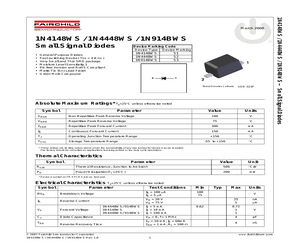
1N914BWS Small Signal Diodes * * * * * * * Device Marking Code Device Type Device Marking 1N4148WS S1 1N4448WS S2 1N914BWS S3 General Purpose Diodes Fast switching Device( TRR < 4.0 ns ) Very Small and Thin SMD package Moisture Level Sensitivity 1 Pb-free Version and RoHS Compliant Matte Tin (Sn) Lead Finish Green Mold Compound *Band Denotes Cathode SOD-323F Absolute Maximum Ratings* Ta=25C unless otherwise noted Symbol Parameter Value Units VRSM Non-Repetitive Peak Reverse Voltage 100 V VRRM Repetitive Peak Reverse Voltage 75 V I FRM Repetitive Peak Forward Current 300 mA IO Continuous Forward Current 150 mA TJ Operating Junction Temperature Range +150 C TSTG Storage Temperature Range -55 to +150 C * These ratings are limiting values above which the serviceability of any semiconductor device may be impaired. The factory should be consulted on applications involving pulsed or low duty cycle operations. Thermal Characteristics Value Unit RJA Symbol Thermal Resistance, Junction to Ambi
 6 Pages, 114 KB, Original
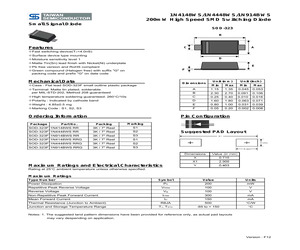
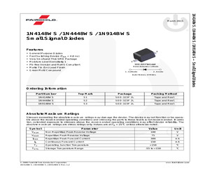
1N914BWS Small Signal Diodes Features * * * * * * * 2 General Purpose Diodes Fast Switching Device (TRR < 4.0 ns) Very Small and Thin SMD Package Moisture Level Sensitivity 1 Pb-free Version and RoHS Compliant Matte Tin (Sn) Lead Finish Green Mold Compound 1 SOD-323 Flat Lead Band Indicates Cathode 1. Cathode 2. Anode ELECTRICAL SYMBOL Ordering Information Part Number Top Mark Package Packing Method 1N4148WS S1 SOD-323F 2L Tape and Reel 1N4448WS S2 SOD-323F 2L Tape and Reel 1N914BWS S3 SOD-323F 2L Tape and Reel Absolute Maximum Ratings Stresses exceeding the absolute maximum ratings may damage the device. The device may not function or be operable above the recommended operating conditions and stressing the parts to these levels is not recommended. In addition, extended exposure to stresses above the recommended operating conditions may affect device reliability. The absolute maximum ratings are stress ratings only. Values are at TA = 25C unless otherwise noted. Symbol Parameter Valu
 5 Pages, 217 KB, Original
1N914BWS Small Signal Diodes Features * * * * * * * 2 General Purpose Diodes Fast Switching Device (TRR < 4.0 ns) Very Small and Thin SMD Package Moisture Level Sensitivity 1 Pb-free Version and RoHS Compliant Matte Tin (Sn) Lead Finish Green Mold Compound 1 SOD-323 Flat Lead Band Indicates Cathode 1. Cathode 2. Anode ELECTRICAL SYMBOL Ordering Information Part Number Top Mark Package Packing Method 1N4148WS S1 SOD-323F 2L Tape and Reel 1N4448WS S2 SOD-323F 2L Tape and Reel 1N914BWS S3 SOD-323F 2L Tape and Reel Absolute Maximum Ratings Stresses exceeding the absolute maximum ratings may damage the device. The device may not function or be operable above the recommended operating conditions and stressing the parts to these levels is not recommended. In addition, extended exposure to stresses above the recommended operating conditions may affect device reliability. The absolute maximum ratings are stress ratings only. Values are at TA = 25C unless otherwise noted. Symbol Parameter Valu
 6 Pages, 222 KB, Original
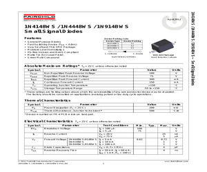
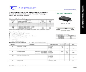
1N914BWS 200mW High Speed SMD Switching Diode Small Signal Diode SOD-323 B Features A C Fast switching device(Trr<4.0nS) Surface device type mounting D Moisture sensitivity level 1 Matte Tin(Sn) lead finish with Nickel(Ni) underplate E Pb free version and RoHS compliant Green compound (Halogen free) with suffix "G" on packing code and prefix "G" on date code F Mechanical Data Unit (mm) Unit (inch) Min Max Min Terminal: Matte tin plated, solderable per MIL-STD-202, Method 208 guaranteed A 1.15 1.35 0.045 0.053 B 2.30 2.70 0.091 0.106 High temperature soldering guaranteed: 260C/10s C 0.25 0.40 0.010 0.016 Polarity : Indicated by cathode band D 1.60 1.80 0.063 0.071 Weight : 4.850.5 mg E 0.80 1.00 0.031 0.039 Marking Code : S1, S2, S3 F 0.05 0.20 0.002 0.008 Dimensions Case : Flat lead SOD-323F small outline plastic package Ordering Information Pin Configuration Packing Marking SOD-323F 1N4148WS RR 3K / 7" Reel S1 SOD-323F 1N4448WS RR 3K / 7" Reel S2 SOD-323F 1N914BWS RR 3K / 7" Reel S3
 3 Pages, 331 KB, Original
1N914BWS Small Signal Diodes Features * * * * * * * Device Marking Code General Purpose Diodes Fast Switching Device (TRR < 4.0ns) Very Small and Thin SMD Package Moisture Level Sensitivity 1 Pb-free Version and RoHS Compliant Matte Tin (Sn) Lead Finish Green Mold Compound Absolute Maximum Ratings* Device Type Device Marking 1N4148WS S1 1N4448WS S2 S3 1N914BWS 1. Cathode 2. Anode 1 SOD-323 Flat Lead Band Indicates Cathode ELECTRICAL SYMBOL Ta = 25C unless otherwise noted Parameter Symbol 2 Value Units VRSM Non-Repetitive Peak Reverse Voltage 100 V VRRM Repetitive Peak Reverse Voltage 75 V IFRM Repetitive Peak Forward Current 300 mA IO Continuous Forward Current 150 mA TJ Operating Junction Temperature +150 C -55 to +150 C TSTG Storage Temperature Range * These ratings are limiting values above which the serviceability of any semiconductor device may be impaired. The factory should be consulted on applications involving pulsed or low duty cycle operations. Thermal Characteristics Valu
 4 Pages, 235 KB, Original
1N914BWS Small Signal Diodes Features * * * * * * * 2 General Purpose Diodes Fast Switching Device (TRR < 4.0 ns) Very Small and Thin SMD Package Moisture Level Sensitivity 1 Pb-free Version and RoHS Compliant Matte Tin (Sn) Lead Finish Green Mold Compound 1 SOD-323 Flat Lead Band Indicates Cathode 1. Cathode 2. Anode ELECTRICAL SYMBOL Ordering Information Part Number Top Mark Package Packing Method 1N4148WS S1 SOD-323F 2L Tape and Reel 1N4448WS S2 SOD-323F 2L Tape and Reel 1N914BWS S3 SOD-323F 2L Tape and Reel Absolute Maximum Ratings Stresses exceeding the absolute maximum ratings may damage the device. The device may not function or be operable above the recommended operating conditions and stressing the parts to these levels is not recommended. In addition, extended exposure to stresses above the recommended operating conditions may affect device reliability. The absolute maximum ratings are stress ratings only. Values are at TA = 25C unless otherwise noted. Symbol Parameter Valu
 6 Pages, 222 KB, Original
uctor was negligent regarding the design or manufacture of the part. ON Semiconductor is an Equal Opportunity/Affirmative Action Employer. This literature is subject to all applicable copyright laws and is not for resale in any manner. 1N4148WS, 1N4448WS, 1N914BWS Small Signal Diodes Features * * * * * * * General Purpose Diodes Fast Switching Device (TRR < 4.0 ns) Very Small and Thin SMD Package Moisture Level Sensitivity 1 Matte Tin (Sn) Lead Finish Green Mold Compound Pb-free Version and RoHS Compliant www.onsemi.com T 2 ABSOLUTE MAXIMUM RATINGS 1 Symbol Value Unit Non-Repetitive Peak Reverse Voltage VRSM 100 V SOD-323 Flat Lead CASE 477AB Repetitive Peak Reverse Voltage VRRM 75 V Band Indicates Cathode Repetitive Peak Forward Current IFRM 300 mA IO 150 mA Parameter Continuous Forward Current Non-repetitive Peak Forward Surge Current Pulse Width = 1.0 s Pulse Width = 1.0 ms Operating Junction Temperature Storage Temperature Range IFSM ELECTRICAL SYMBOL A 1.0 4.0 (1) Cathode TJ +150 C TSTG -55
 6 Pages, 170 KB, Original
1N914BWS 200mW High Speed SMD Switching Diode Small Signal Diode SOD-323F B Features C A Fast switching device(Trr<4.0nS) Surface device type mounting D Moisture sensitivity level 1 Matte Tin(Sn) lead finish with Nickel(Ni) underplate E Pb free version and RoHS compliant Green compound (Halogen free) with suffix "G" on packing code and prefix "G" on date code F Mechanical Data Unit (mm) Dimensions Case : Flat lead SOD-323 small outline plastic package Unit (inch) Min Max Terminal: Matte tin plated, lead free., solderable per MIL-STD-202, Method 208 guaranteed A 1.15 1.35 0.045 0.053 B 2.30 2.70 0.091 0.106 High temperature soldering guaranteed: 260C/10s C 0.25 0.40 0.010 0.016 Polarity : Indicated by cathode band D 1.60 1.80 0.063 0.071 Weight : 4.850.5 mg E 0.80 1.00 0.031 0.039 Marking Code : S1, S2, S3 F 0.05 0.20 0.002 0.008 Ordering Information Packing Marking 3K / 7" Reel S1 SOD-323F 1N4448WS RR 3K / 7" Reel S2 SOD-323F 1N9148BWS RR 3K / 7" Reel S3 SOD-323F 1N4148WS RRG 3K / 7" Reel S1 SOD-
 3 Pages, 126 KB, Original
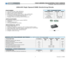
1N914BWS Taiwan Semiconductor 200mW High Speed SMD Switching Diode FEATURES KEY PARAMETERS Low power loss, high efficiency Ideal for automated placement High surge current capability Moisture sensitivity level: level 1, per J-STD-020 Compliant to RoHS directive 2011/65/EU and in accordance to WEEE 2002/96/EC Halogen-free according to IEC 61249-2-21 PARAMETER VALUE UNIT VRRM 100 V VF at IF=100mA 1.0 V TJ MAX. 150 C Package SOD-323F Configuration Single die APPLICATIONS Switching mode power supply (SMPS) Adapters Lighting application On-board DC/DC converter MECHANICAL DATA Case: SOD-323F Molding compound meets UL 94 V-0 flammability rating Terminal: Matte tin plated leads, solderable per J-STD-002 Meet JESD 201 class 1A whisker test Polarity: Indicated by cathode band Weight: 4.85 0.5 mg ABSOLUTE MAXIMUM RATINGS (TA = 25C unless otherwise noted) PARAMETER SYMBOL Marking code on the device Power dissipation 1N4148 1N4448 1N914B WS WS WS S1 S2 S3 UNIT PD 200 VRRM IF 100 V Forward current Non-repetit
 5 Pages, 162 KB, Original
orward Current 150 mA TJ IO These ratings are limiting values above which the serviceability of the diode may be impaired. Specification Features: Fast Switching Device (T RR <4.0 nS) DEVICE MARKING CODE: Device Type Device Marking 1N4148WS S1 1N4448WS S2 1N914BWS S3 General Purpose Diodes Flat Lead SOD-323 Small Outline Plastic Package Surface Device Type Mounting RoHS Compliant Green EMC Matte Tin(Sn) Lead Finish Band Indicates Cathode Electrical Characteristics TA = 25C unless otherwise noted Parameter Symbol Limits Test Condition Min BV Breakdown Voltage IR Reverse Leakage Current VF Forward Voltage IR=100A 100 IR=5A 75 VR=20V VR=75V 1N4448WS, 1N914BWS TC1N4448WS, 1N4148WS 1N4448WS, 1N914BWS TRR Reverse Recovery Time IF=5mA 0.62 Unit Max Volts 25 nA 5 A 0.72 IF=10mA 1.0 IF=100mA 1.0 Volts IF=10mA IR=60mA 4 nS 4 pF RL=100 IRR=1mA C Capacitance VR=0V, f=1M HZ Oct 2008 Release, Revision E Page 1 1N4148WS/1N4448WS/1N914BWS TAK CHEONG TAK CHEONG (R) SEMICONDU
 4 Pages, 403 KB, Original
1N914BWS S3 Small Outline Flat Lead Plastic Package Fast Switching Diode Absolute Maximum Ratings Symbol PD TSTG TA = 25C unless otherwise noted Parameter Power Dissipation Units 200 mW -65 to +150 C Operating Junction Temperature +150 C VRSM Non-Repetitive Peak Reverse Voltage 100 V VRRM Repetitive Peak Reverse Voltage 75 V IFRM Repetitive Peak Forward Current 300 mA Continuous Forward Current 150 mA TJ IO Storage Temperature Range Value SOD-323 Flat Lead These ratings are limiting values above which the serviceability of the diode may be impaired. Specification Features: Fast Switching Device (TRR <4.0 nS) General Purpose Diodes Flat Lead SOD-323 Small Outline Plastic Package Cathode Anode Surface Device Type Mounting ELECTRICAL SYMBOL RoHS Compliant Matte Tin(Sn) Lead Finish Band Indicates Cathode Electrical Characteristics Symbol TA = 25C unless otherwise noted Parameter Limits Test Condition Min BV Breakdown Voltage IR Reverse Leakage Current VF Forward Voltage IR=100A 100 IR=5A 75 Volts VR=
 2 Pages, 88 KB, Original
1N914BWS 200mW High Speed SMD Switching Diode Small Signal Diode SOD-323F B Features C A Fast switching device(Trr<4.0nS) Surface device type mounting D Moisture sensitivity level 1 Matte Tin(Sn) lead finish with Nickel(Ni) underplate E Pb free version and RoHS compliant Green compound (Halogen free) with suffix "G" on packing code and prefix "G" on date code F Mechanical Data Unit (mm) Dimensions Case : Flat lead SOD-323F small outline plastic package Unit (inch) Min Max Terminal: Matte tin plated, solderable per MIL-STD-202, Method 208 guaranteed A 1.15 1.35 0.045 0.053 B 2.30 2.70 0.091 0.106 High temperature soldering guaranteed: 260C/10s C 0.25 0.40 0.010 0.016 Polarity : Indicated by cathode band D 1.60 1.80 0.063 0.071 Weight : 4.850.5 mg E 0.80 1.00 0.031 0.039 Marking Code : S1, S2, S3 F 0.05 0.20 0.002 0.008 Ordering Information Packing Marking 3K / 7" Reel S1 SOD-323F 1N4448WS RR 3K / 7" Reel S2 SOD-323F 1N914BWS RR 3K / 7" Reel S3 SOD-323F 1N4148WS RRG 3K / 7" Reel S1 SOD
 3 Pages, 167 KB, Original
uctor was negligent regarding the design or manufacture of the part. ON Semiconductor is an Equal Opportunity/Affirmative Action Employer. This literature is subject to all applicable copyright laws and is not for resale in any manner. 1N4148WS, 1N4448WS, 1N914BWS Small Signal Diodes Features * * * * * * * General Purpose Diodes Fast Switching Device (TRR < 4.0 ns) Very Small and Thin SMD Package Moisture Level Sensitivity 1 Matte Tin (Sn) Lead Finish Green Mold Compound Pb-free Version and RoHS Compliant www.onsemi.com T 2 ABSOLUTE MAXIMUM RATINGS 1 Symbol Value Unit Non-Repetitive Peak Reverse Voltage VRSM 100 V SOD-323 Flat Lead CASE 477AB Repetitive Peak Reverse Voltage VRRM 75 V Band Indicates Cathode Repetitive Peak Forward Current IFRM 300 mA IO 150 mA Parameter Continuous Forward Current Non-repetitive Peak Forward Surge Current Pulse Width = 1.0 s Pulse Width = 1.0 ms Operating Junction Temperature Storage Temperature Range IFSM ELECTRICAL SYMBOL A 1.0 4.0 (1) Cathode TJ +150 C TSTG -55
 6 Pages, 153 KB, Original
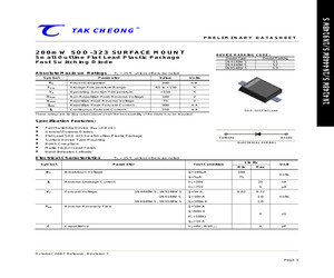
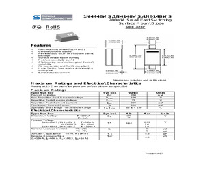
1N914BWS 200mW Small Fast Switching Surface Mount Diode Pb RoHS SOD-323F COMPLIANCE Features Fast switching device(TRR<4.0nS) General purpose diodes Flat lead SOD-323F small outline plastic package Surface device type mounting Moisture sensitivity level 1 Clip bonding construction, good thermal capability Pb free version and RoHS compliant Matte Tin(Sn) lead finish with Nickel(Ni) underplate Band indicates cathode Dimensions in inches and (millimeters) Maximum Ratings and Electrical Characteristics Rating at 25oC ambient temperature unless otherwise specified. Maximum Ratings Type Number Power Dissipation Non-Repetitive Peak Reverse Voltage Repetitive Peak Reverse Voltage Repetitive Peak Forward Current Continuous Forward Current Operating and Storage Temperature Range Symbol Pd VRSM VRRM IFRM Io TJ, TSTG Value Units mW V V mA mA O C 200 100 75 300 150 -65 to + 150 Electrical Characteristics Type Number Breakdown Voltage IR=100uA IR=5uA Forward Voltage 1N4448WS, 1N914BWS IF=5.0mA 1N4
 3 Pages, 82 KB, Original
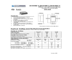
1N914BWS 200mW Small Fast Switching Surface Mount Diode Pb RoHS SOD-323F COMPLIANCE Features Fast switching device(TRR<4.0nS) General purpose diodes Flat lead SOD-323F small outline plastic package Surface device type mounting Moisture sensitivity level 1 Clip bonding construction, good thermal capability Pb free version and RoHS compliant Matte Tin(Sn) lead finish with Nickel(Ni) underplate Band indicates cathode Dimensions in inches and (millimeters) Maximum Ratings and Electrical Characteristics Rating at 25oC ambient temperature unless otherwise specified. Maximum Ratings Type Number Power Dissipation Non-Repetitive Peak Reverse Voltage Repetitive Peak Reverse Voltage Repetitive Peak Forward Current Continuous Forward Current Operating and Storage Temperature Range Symbol Pd VRSM VRRM IFRM Io TJ, TSTG Value Units mW V V mA mA O C 200 100 75 300 150 -65 to + 150 Electrical Characteristics Type Number Breakdown Voltage IR=100uA IR=5uA Forward Voltage 1N4448WS, 1N914BWS IF=5.0mA 1N4
 3 Pages, 441 KB, Original