C5 150pF R24 15k TP9 15 16 18 17 19 20 21 22 23 24 25 26 R25 1k A B J11 MC145423 VDD TP2 16 R26 1k TI+ TG TI- 19 18 17 PI 3 PO4 PO+ 5 PDL 10 RO2 MU/A VDD 6 TX 15 C9 150pF R27 15k U4A 1 20 11 9 12 14 13 7 8 VDD MCLK VSS TP10 C8 0.1F TP24 C4 0.1F VAGREF D6 1N914B D4 RX R2 5k D2 SDO1 SDO2 YELLOW TX D3 Q1 TPDT TP7 9 8 7 6 R15 110 P2N2907A D7 1N914B R11 110 D5 1N914B 1N914B VDD 1N914B R14 110 VDD R10 110 BCLKR VAG D1 R1 5k 1N914B VDD BCLKT DT FST FSR DR R8 10k TP3 TP5 MC145484 C29 0.1F EN2-TE2/SIE/B1B2 EN1-TE1 MSI/Tone CCI/Xtal n LI Sens/2.048MHz TDC-RDC/Xtal Out RE1/CLKOut RX RE2/BCLK LO1 LO2 VDD 2828 27 Master/Slave C28 0.1F C43 0.1F R18 20k R21 200k VDD 13 Mod Tri/Sq 14 PDL SE/(MU/A) 12 SDO1 10 SDO2 11 Frame 10/20 8 SDCLK/8kHz 9 R20 3k R17 3k TP8 R22 1k S1 R19 1k White a REC White b J2 TP1 TP27 R4 10k R3 10k R5 10k R6 10k BNC J22 S1 R9 332 R13 1K B A B A P1358A SDI1 SDI2 R7 10k J25 RING TIP CLK1 S2 RE2 - 4 SDO2 - 18 SDO1 - 12 VD - 24
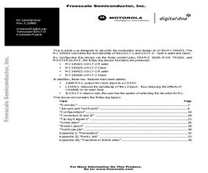 40 Pages, 505 KB, Original
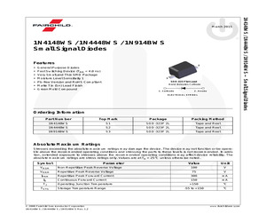
1N914BWS Small Signal Diodes Features * * * * * * * 2 General Purpose Diodes Fast Switching Device (TRR < 4.0 ns) Very Small and Thin SMD Package Moisture Level Sensitivity 1 Pb-free Version and RoHS Compliant Matte Tin (Sn) Lead Finish Green Mold Compound 1 SOD-323 Flat Lead Band Indicates Cathode 1. Cathode 2. Anode ELECTRICAL SYMBOL Ordering Information Part Number Top Mark Package Packing Method 1N4148WS S1 SOD-323F 2L Tape and Reel 1N4448WS S2 SOD-323F 2L Tape and Reel 1N914BWS S3 SOD-323F 2L Tape and Reel Absolute Maximum Ratings Stresses exceeding the absolute maximum ratings may damage the device. The device may not function or be operable above the recommended operating conditions and stressing the parts to these levels is not recommended. In addition, extended exposure to stresses above the recommended operating conditions may affect device reliability. The absolute maximum ratings are stress ratings only. Values are at TA = 25C unless otherwise noted. Symbol Parameter Valu
 6 Pages, 222 KB, Original
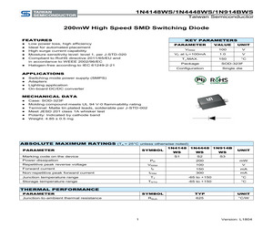
1N914BWS Taiwan Semiconductor 200mW High Speed SMD Switching Diode FEATURES KEY PARAMETERS Low power loss, high efficiency Ideal for automated placement High surge current capability Moisture sensitivity level: level 1, per J-STD-020 Compliant to RoHS directive 2011/65/EU and in accordance to WEEE 2002/96/EC Halogen-free according to IEC 61249-2-21 PARAMETER VALUE UNIT VRRM 100 V VF at IF=100mA 1.0 V TJ MAX. 150 C Package SOD-323F Configuration Single die APPLICATIONS Switching mode power supply (SMPS) Adapters Lighting application On-board DC/DC converter MECHANICAL DATA Case: SOD-323F Molding compound meets UL 94 V-0 flammability rating Terminal: Matte tin plated leads, solderable per J-STD-002 Meet JESD 201 class 1A whisker test Polarity: Indicated by cathode band Weight: 4.85 0.5 mg ABSOLUTE MAXIMUM RATINGS (TA = 25C unless otherwise noted) PARAMETER SYMBOL Marking code on the device Power dissipation 1N4148 1N4448 1N914B WS WS WS S1 S2 S3 UNIT PD 200 VRRM IF 100 V Forward curren
 5 Pages, 162 KB, Original
35V .01F 100V .033F 400V .22F 1KV .001F 1KV .1F 50V 1F 50V N.P. .0047F 1KV .1F 50V 47F 16V DIODES R4 C9 R27 2N6027 3052 MOC S4015L S4015L LM358 IC 275V G-MOV C11 R10 R28 Q3 R24 ............... .062 5W R18 -8 P1 D1 D2 D3 D4 D5 D6 D7 D8 D9 D10 1N4005 1N4005 1N914B 1N5242B 1N4005 1N5233B 1N914B D4015L D4015L D4015L 123D-C CHANGES: MISCELLANEOUS JU1 JU2 PCB P1 (-1 THRU -8) P2 (-2 THRU -6) P3 18GA. SOLID INSULATED WIRE 18GA. SOLID INSULATED WIRE A-4-2033F PRINTED CIRCUIT 8 POS. TERMINAL STRIP 5 POS. FEMALE CONNECTOR 3/16" MALE SPADE PIN 12 D6 Q6 R1 R2 R16 R23 R25 R27 R28 1N914B (reverse direction) DELETE 1K 2W 47 220K 47K 15K 47 47 C1 .01uf 100V +FIELD P1-5 P1-1 D1 1N4005 +12.7V C2 10uf 35V AC1 R1 15K 6W D3 1N914B +12V D4 1N5242B R23 R25 R27 R28 P1-2 2 1 C3 .01uf 100V Q1 2N6027 D2 1N4005 AC2 R3 2.7K R4 2.7K U2-1 3052 MOC .......... 47K .......... 15K .......... 47 .......... 47 123D-C CHANGES: D6 .......... 1N914B Q6 .......... DELETE R1 .......... 1
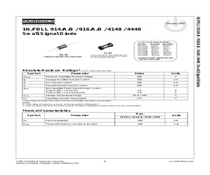
 88 Pages, 3140 KB, Original
semi.com 1N/FDLL 914/A/B / 916/A/B / 4148 / 4448 Small Signal Diode January 2007 Symbol TA=25C unless otherwise noted Parameter VR Breakdown Voltage VF Forward Voltage IR Reverse Leakage CT Total Capacitance 1N916A/B/4448 1N914A/B/4148 trr Test Conditions 1N914B/4448 1N916B 1N914/916/4148 1N914A/916A 1N916B 1N914B/4448 Reverse Recovery Time Min. IR = 100A IR = 5.0A 100 75 IF = 5.0mA IF = 5.0mA IF = 10mA IF = 20mA IF = 20mA IF = 100mA 620 630 Max. Units V V 720 730 1.0 1.0 1.0 1.0 mV mV V V V V VR = 20V VR = 20V, TA = 150C VR = 75V 25 50 5.0 nA A A VR = 0, f = 1.0MHz VR = 0, f = 1.0MHz 2.0 4.0 pF pF IF = 10mA, VR = 6.0V (600mA) Irr = 1.0mA, RL = 100 4.0 ns * Non-recurrent square wave PW = 8.3ms Typical Characteristics 120 160 o o Ta= 25 C [nA] 150 100 140 80 Reverse Current, I Reverse Voltage, V R R [V] Ta=25 C 130 120 60 40 20 110 1 2 3 5 10 20 30 50 0 100 10 20 30 50 Reverse Voltage, VR [V] Reverse Current, IR [uA] 70 100 GENERAL RULE: The Reverse Current of a diode will approximate
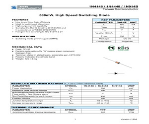
 7 Pages, 200 KB, Original
1N914B Taiwan Semiconductor 500mW, High Speed Switching Diode FEATURES KEY PARAMETERS Low power loss, high efficiency Ideal for automated placement High surge current capability Compliant to RoHS directive 2011/65/EU and in accordance to WEEE 2002/96/EC Halogen-free according to IEC 61249-2-21 APPLICATIONS Switching mode power supply (SMPS) PARAMETER VALUE UNIT IF 150 mA VRRM 100 V IFSM 2 A VF at IF=100mA 1 V TJ MAX 150 C Package DO-35 Configuration Singal die MECHANICAL DATA Case: DO-35 Packing code with suffix "G" means green compound (halogen-free) Terminal: Matte tin plated leads, solderable per J-STD-002 Polarity: Indicated by cathode band Weight: 125 4 mg ABSOLUTE MAXIMUM RATINGS (TA = 25C unless otherwise noted) PARAMETER Power dissipation SYMBOL 1N4148 1N4448 1N914B UNIT PD 500 mW VRRM 100 V IFSM 2 A Forward current IFM IF 450 150 mA mA Junction temperature range TJ -65 to +150 C Storage temperature range TSTG -65 to +150 C SYMBOL TYP UNIT RJA 240 C/W Repetitive peak reverse
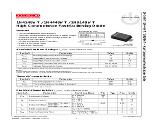
 5 Pages, 170 KB, Original
tor was negligent regarding the design or manufacture of the part. ON Semiconductor is an Equal Opportunity/Affirmative Action Employer. This literature is subject to all applicable copyright laws and is not for resale in any manner. 1N4148WT / 1N4448WT / 1N914BWT High Conductance Fast Switching Diode Features * * * * * * * Device Marking Code Device Type Device Marking 1N4148WT E1 1N4448WT E2 1N914BWT E3 Fast Switching Diode (Trr <4.0nsec) Flat Lead, Surface Mount Device Under 0.70mm Height Extremely Small Outline Plastic Package SOD523F Moisture Level Sensitivity 1 Pb-free Version and RoHS Compliant Matte Tin (Sn) Lead Finish Green Mold Compound Absolute Maximum Ratings* Symbol Cathode Anode ELECTRICAL SYMBOL SOD-523F Band Indicates Cathode TA=25C unless otherwise noted Parameter Value Units VRSM Non-Repetitive Peak Reverse Voltage 75 V VRRM Repetitive Peak Reverse Voltage 75 V I FRM Repetitive Peak Forward Current 300 mA Operating Junction Temperature Range -55 to +150 C Storage T
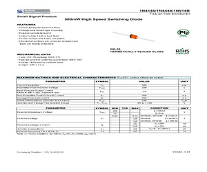
 8 Pages, 292 KB, Original
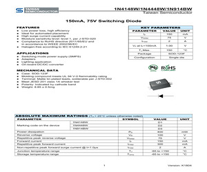
1N914B Taiwan Semiconductor Small Signal Product 500mW High Speed Switching Diode FEATURES - Fast switching device(Trr<4.0nS) - Through-hole device type mounting - Moisture sensitivity level 1 - Solder hot dip Tin(Sn) lead finish - Pb free version and RoHS compliant - All external surfaces are corrosion resistant and leads are readily solderable DO-35 HERMETICALLY SEALED GLASS MECHANICAL DATA - Case : DO-35 package (SOD-27) - High temperature soldering guaranteed: 260C/10s - Polarity : Indicated by cathode band - Weight : 109 4 mg MAXIMUM RATINGS AND ELECTRICAL CHARACTERISTICS (TA=25 unless otherwise noted) PARAMETER SYMBOL VALUE UNIT Power Dissipation Repetitive Peak Reverse Voltage PD VRRM 500 100 mW V Peak Forward Surge Current Pluse Width = 1S, Square Wave IFSM 2.0 A Non-Repetitive Peak Forward Current IFM 450 mA Average Forward Current IO 150 Thermal Resistance (Junction to Ambient) RJA 240 Junction and Storage Temperature Range TJ , TSTG -65 to + 150 PARAMETER SYMBOL Reverse Breakdown Volta
 5 Pages, 448 KB, Original
1N914BWT High Conductance Fast Switching Diode Features * * * * * * * Device Marking Code Device Type Device Marking 1N4148WT E1 1N4448WT E2 1N914BWT E3 Fast Switching Diode (Trr <4.0nsec) Flat Lead, Surface Mount Device Under 0.70mm Height Extremely Small Outline Plastic Package SOD523F Moisture Level Sensitivity 1 Pb-free Version and RoHS Compliant Matte Tin (Sn) Lead Finish Green Mold Compound Absolute Maximum Ratings* Symbol Cathode Anode ELECTRICAL SYMBOL SOD-523F Band Indicates Cathode TA=25C unless otherwise noted Parameter Value Units VRSM Non-Repetitive Peak Reverse Voltage 75 V VRRM Repetitive Peak Reverse Voltage 75 V I FRM Repetitive Peak Forward Current 300 mA Operating Junction Temperature Range -55 to +150 C Storage Temperature Range -55 to +150 C Value Units Power Dissipation (TC=25C) 200 mW Thermal Resistance, Junction to Ambient 500 C/W TJ TSTG * These ratings are limiting values above which the serviceability of any semiconductor device may be impaired. NOTES: 1) T
 7 Pages, 177 KB, Original
1N914BWS Small Signal Diodes Features * * * * * * * 2 General Purpose Diodes Fast Switching Device (TRR < 4.0 ns) Very Small and Thin SMD Package Moisture Level Sensitivity 1 Pb-free Version and RoHS Compliant Matte Tin (Sn) Lead Finish Green Mold Compound 1 SOD-323 Flat Lead Band Indicates Cathode 1. Cathode 2. Anode ELECTRICAL SYMBOL Ordering Information Part Number Top Mark Package Packing Method 1N4148WS S1 SOD-323F 2L Tape and Reel 1N4448WS S2 SOD-323F 2L Tape and Reel 1N914BWS S3 SOD-323F 2L Tape and Reel Absolute Maximum Ratings Stresses exceeding the absolute maximum ratings may damage the device. The device may not function or be operable above the recommended operating conditions and stressing the parts to these levels is not recommended. In addition, extended exposure to stresses above the recommended operating conditions may affect device reliability. The absolute maximum ratings are stress ratings only. Values are at TA = 25C unless otherwise noted. Symbol Parameter Valu
 5 Pages, 217 KB, Original
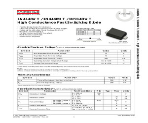
tor was negligent regarding the design or manufacture of the part. ON Semiconductor is an Equal Opportunity/Affirmative Action Employer. This literature is subject to all applicable copyright laws and is not for resale in any manner. 1N4148WT / 1N4448WT / 1N914BWT High Conductance Fast Switching Diode Features * * * * * * * Device Marking Code Device Type Device Marking 1N4148WT E1 1N4448WT E2 1N914BWT E3 Fast Switching Diode (Trr <4.0nsec) Flat Lead, Surface Mount Device Under 0.70mm Height Extremely Small Outline Plastic Package SOD523F Moisture Level Sensitivity 1 Pb-free Version and RoHS Compliant Matte Tin (Sn) Lead Finish Green Mold Compound Absolute Maximum Ratings* Symbol Cathode Anode ELECTRICAL SYMBOL SOD-523F Band Indicates Cathode TA=25C unless otherwise noted Parameter Value Units VRSM Non-Repetitive Peak Reverse Voltage 75 V VRRM Repetitive Peak Reverse Voltage 75 V I FRM Repetitive Peak Forward Current 300 mA Operating Junction Temperature Range -55 to +150 C Storage T
 8 Pages, 275 KB, Original
1N914BWT High Conductance Fast Switching Diode Features * * * * * * * Device Marking Code Device Type Device Marking 1N4148WT E1 1N4448WT E2 1N914BWT E3 Fast Switching Diode (Trr <4.0nsec) Flat Lead, Surface Mount Device Under 0.70mm Height Extremely Small Outline Plastic Package SOD523F Moisture Level Sensitivity 1 Pb-free Version and RoHS Compliant Matte Tin (Sn) Lead Finish Green Mold Compound Absolute Maximum Ratings* Symbol Cathode Anode ELECTRICAL SYMBOL SOD-523F Band Indicates Cathode TA=25C unless otherwise noted Parameter Value Units VRSM Non-Repetitive Peak Reverse Voltage 75 V VRRM Repetitive Peak Reverse Voltage 75 V I FRM Repetitive Peak Forward Current 300 mA Operating Junction Temperature Range -55 to +150 C Storage Temperature Range -55 to +150 C Value Units Power Dissipation (TC=25C) 200 mW Thermal Resistance, Junction to Ambient 500 C/W TJ TSTG * These ratings are limiting values above which the serviceability of any semiconductor device may be impaired. NOTES: 1) T
 6 Pages, 176 KB, Original
1N914BWT High Conductance Fast Switching Diode * * * * * * * Fast Switching Diode (Trr <4.0nsec) Flat Lead, Surface Mount Device under 0.70mm Height Extremely Small Outline Plastic Package SOD523F Moisture Level Sensitivity 1 Pb-free Version and RoHS Compliant Matte Tin (Sn) Lead Finish Green Mold Compound Device Marking Code Device Type Device Marking 1N4148WT E1 1N4448WT E2 1N914BWT E3 SOD-523F Band Indicates Cathode* Absolute Maximum Ratings* Ta=25C unless otherwise noted Symbol Parameter Value Units VRSM Non-Repetitive Peak Reverse Voltage 75 V VRRM Repetitive Peak Reverse Voltage 75 V I FRM Repetitive Peak Forward Current 300 mA TJ Operating Junction Temperature Range -55 to +150 C TSTG Storage Temperature Range -55 to +150 C * These ratings are limiting values above which the serviceability of any semiconductor device may be impaired. NOTES: 1) These ratings are based on a maximum junction temperature of 150 degrees C. 2) These are steady state limits. The factory should be con
 6 Pages, 109 KB, Original
1N914BW Taiwan Semiconductor 150mA, 75V Switching Diode FEATURES KEY PARAMETERS Low power loss, high efficiency Ideal for automated placement High surge current capability Moisture sensitivity level: level 1, per J-STD-020 Compliance to RoHS directive 2011/65/EU and in accordance to WEEE 2002/96/EC Halogen-free according to IEC 61249-2-21 PARAMETER VALUE UNIT IF 150 mA VRRM 75 V IFSM 2 A VF at IF=100mA 1.00 V TJ Max. 150 C APPLICATIONS Switching mode power supply (SMPS) Adapters Lighting application On-board DC/DC converter Package SOD-123F Configuration Single die MECHANICAL DATA Case: SOD-123F Molding compound meets UL 94 V-0 flammability rating Terminal: Matte tin plated leads, solderable per J-STD-002 Meet JESD 201 class 1A whisker test Polarity: Indicated by cathode band Weight: 8.85 0.5mg ABSOLUTE MAXIMUM RATINGS (TA = 25C unless otherwise noted) PARAMETER Marking code on the device SYMBOL VALUE 1N4148W D1 1N4448W D2 1N914BW D3 UNIT Power dissipation PD 400 mW Reverse voltage V
 5 Pages, 164 KB, Original